EVAL-ADUC824QS Analog Devices Inc, EVAL-ADUC824QS Datasheet - Page 41
EVAL-ADUC824QS
Manufacturer Part Number
EVAL-ADUC824QS
Description
KIT DEV FOR ADUC824 QUICK START
Manufacturer
Analog Devices Inc
Series
QuickStart™ Kitr
Type
8052-corer
Datasheet
1.EVAL-ADUC824QSZ.pdf
(68 pages)
Specifications of EVAL-ADUC824QS
Contents
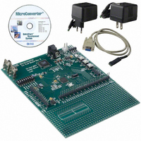
Evaluation Board, Power Supply, Cable, Software and Documentation
For Use With/related Products
ADuC824
Lead Free Status / RoHS Status
Contains lead / RoHS non-compliant


USER INTERFACE TO OTHER ON-CHIP ADuC824
PERIPHERALS
The following section gives a brief overview of the various peripher-
als also available on-chip. A summary of the SFRs used to control
and configure these peripherals is also given.
DAC
The ADuC824 incorporates a 12-bit, voltage output DAC on-chip.
It has a rail-to-rail voltage output buffer capable of driving
DACCON
SFR Address
Power-On Default Value
Bit Addressable
Bit
7
6
5
4
3
2
1
0
DACH/L
Function
SFR Address
Power-On Default Value
Bit Addressable
The 12-bit DAC data should be written into DACH/L right-justified such that DACL contains the lower eight bits, and the lower
nibble of DACH contains the upper four bits.
—
Name
—
—
—
DACPIN
DAC8
DACRN
DACCLR
DACEN
—
Description
Reserved for Future Use
Reserved for Future Use
Reserved for Future Use
DAC Output Pin Select
Set by user to direct the DAC output to Pin 12 (P1.7/AIN4/DAC).
Cleared by user to direct the DAC output to Pin 3 (P1.2/DAC/IEXC1).
DAC 8-Bit Mode Bit
Set by user to enable 8-bit DAC operation. In this mode the 8-bits in DACL SFR are routed to the
8 MSBs of the DAC and the 4 LSBs of the DAC are set to zero.
Cleared by user to operate the DAC in its normal 12-bit mode of operation.
DAC Output Range Bit
Set by user to configure DAC range of 0 –AV
Cleared by user to configure DAC range 0 – 2.5 V.
DAC Clear Bit
Set to ‘1’ by user to enable normal DAC operation.
Cleared to ‘0’ by used to reset DAC data registers DAC1/H to zero.
DAC Enable Bit
Set to ‘1’ by user to enable normal DAC operation.
Cleared to ‘0’ by used to power-down the DAC.
DAC Control Register
No
DAC Data Register
DAC Data Registers, written by user to update the DAC output.
DACH (DAC Data High Byte) –>FCH
FDH
00H
DACL (DAC Data Low Byte) –>FBH
00H
No
—
Table XVI. DACCON SFR Bit Designations
DACPIN
10 kΩ/100 pF. It has two selectable ranges, 0 V to V
nal bandgap 2.5 V reference) and 0 V to AV
12-bit or 8-bit mode. The DAC has a control register, DACCON,
and two data registers, DACH/L. The DAC output can be
programmed to appear at Pin 3 or Pin 12. It should be noted
that in 12-bit mode, the DAC voltage output will be updated as
soon as the DACL data SFR has been written; therefore, the DAC
data register should be updated as DACH first followed by DACL.
–>Both Registers
–>Both Registers
DAC8
DD
.
DACRN
DACCLR
DD
ADuC824
. It can operate in
REF
DACEN
(the inter-
Related parts for EVAL-ADUC824QS
Image
Part Number
Description
Manufacturer
Datasheet
Request
R


Part Number:
Description:
BOARD EVAL FOR SI270X-A
Manufacturer:
Silicon Laboratories Inc
Datasheet:

Part Number:
Description:
BUCK CONV REF DESIGN KIT IP1201
Manufacturer:
International Rectifier
Datasheet:
Part Number:
Description:
BOARD DEMO SYNC DUAL BUCK CNVTER
Manufacturer:
International Rectifier
Datasheet:
Part Number:
Description:
BOARD DEMO SYNC BUCK CONVETER
Manufacturer:
International Rectifier
Datasheet:

Part Number:
Description:
EVALBOARD/EB Omnidirectional microphone - Analog
Manufacturer:
Analog Devices
Datasheet:
Part Number:
Description:
EVALBOARD/EB Omnidirectional microphone - Analog
Manufacturer:
Analog Devices
Datasheet:


Part Number:
Description:
BOARD EVAL LED DRIVER LT3756
Manufacturer:
Linear Technology
Datasheet:

Part Number:
Description:
BOARD EVAL FOR AD7741/7742
Manufacturer:
Analog Devices Inc
Datasheet:

Part Number:
Description:
±1.7g Dual-Axis IMEMS Accelerometer Evaluation Board
Manufacturer:
Analog Devices Inc
Datasheet:

Part Number:
Description:
IC MULTIPLIER ANALOG 8-SOIC T/R
Manufacturer:
Analog Devices Inc
Datasheet:

Part Number:
Description:
IC ANALOG MULTIPLIER 8-DIP
Manufacturer:
Analog Devices Inc
Datasheet:
Part Number:
Description:
IC ANALOG MULTIPLIER 8-SOIC
Manufacturer:
Analog Devices Inc
Datasheet:
Part Number:
Description:
IC ANALOG MULTIPLIER 8-DIP
Manufacturer:
Analog Devices Inc
Datasheet: