EVAL-ADUC824QS Analog Devices Inc, EVAL-ADUC824QS Datasheet - Page 6
EVAL-ADUC824QS
Manufacturer Part Number
EVAL-ADUC824QS
Description
KIT DEV FOR ADUC824 QUICK START
Manufacturer
Analog Devices Inc
Series
QuickStart™ Kitr
Type
8052-corer
Datasheet
1.EVAL-ADUC824QSZ.pdf
(68 pages)
Specifications of EVAL-ADUC824QS
Contents
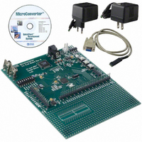
Evaluation Board, Power Supply, Cable, Software and Documentation
For Use With/related Products
ADuC824
Lead Free Status / RoHS Status
Contains lead / RoHS non-compliant


ADuC824
Parameter
LOGIC OUTPUTS (Not Including XTAL2)
POWER SUPPLY MONITOR (PSM)
WATCHDOG TIMER (WDT)
MCU CORE CLOCK RATE
START-UP TIME
FLASH/EE MEMORY RELIABILITY CHARACTERISTICS
POWER REQUIREMENTS
V
V
Floating State Leakage Current
Floating State Output Capacitance
AV
AV
DV
DV
Timeout Period
MCU Clock Rate
At Power-On
From Idle Mode
From Power-Down Mode
After External RESET in Normal Mode
After WDT Reset in Normal Mode
Endurance
Data Retention
Power Supply Voltages
OH
OL
Oscillator Running
Oscillator Powered Down
AV
AV
DV
DV
DD
DD
DD
DD
, Output Low Voltage
, Output High Voltage
Wakeup with INT0 Interrupt
Wakeup with SPI/I
Wakeup with TIC Interrupt
Wakeup with External RESET
Wakeup with External RESET
DD
DD
DD
DD
Trip Point Selection Range
Power Supply Trip Point Accuracy
Trip Point Selection Range
Power Supply Trip Point Accuracy
, 3 V Nominal Operation
, 5 V Nominal Operation
, 3 V Nominal Operation
, 5 V Nominal Operation
15
16
2
2
C Interrupt
13
2
2.63
2.63
ADuC824BS
2.4
2.4
0.4
0.4
0.4
± 10
5
4.63
± 3.5
4.63
± 3.5
0
2000
98.3
12.58
300
1
1
1
1
3.4
0.9
3.3
3.3
100,000
100
2.7
3.6
4.75
5.25
2.7
3.6
4.75
5.25
14
Four Trip Points Selectable in This Range V min
Four Trip Points Selectable in This Range V min
Test Conditions/Comments
V
V
I
I
I
Programmed via TPA1–0 in PSMCON
Programmed via TPD1–0 in PSMCON
Nine Timeout Periods in This Range
Programmed via PRE3–0 in WDCON
Clock Rate Generated via On-Chip PLL
Programmable via CD2–0 Bits in
PLLCON SFR
OSC_PD Bit = 0 in PLLCON SFR
OSC_PD Bit = 1 in PLLCON SFR
Controlled via WDCON SFR
DV
Independently
SINK
SINK
SINK
DD
DD
DD
= 5 V, I
= 3 V, I
= 8 mA, SCLOCK, SDATA/MOSI V max
= 10 mA, P1.0 and P1.1
= 1.6 mA, All Other Outputs
and AV
SOURCE
SOURCE
DD
Can Be Set
= 80 µA
= 20 µA
Unit
V min
V min
V max
V max
µA max
pF typ
V max
% max
V max
% max
ms min
ms max
kHz min
MHz max
ms typ
ms typ
ms typ
ms typ
ms typ
ms typ
sec typ
ms typ
ms typ
Cycles min
Years min
V min
V max
V min
V max
V min
V max
V min
V max
Related parts for EVAL-ADUC824QS
Image
Part Number
Description
Manufacturer
Datasheet
Request
R


Part Number:
Description:
BOARD EVAL FOR SI270X-A
Manufacturer:
Silicon Laboratories Inc
Datasheet:

Part Number:
Description:
BUCK CONV REF DESIGN KIT IP1201
Manufacturer:
International Rectifier
Datasheet:
Part Number:
Description:
BOARD DEMO SYNC DUAL BUCK CNVTER
Manufacturer:
International Rectifier
Datasheet:
Part Number:
Description:
BOARD DEMO SYNC BUCK CONVETER
Manufacturer:
International Rectifier
Datasheet:

Part Number:
Description:
EVALBOARD/EB Omnidirectional microphone - Analog
Manufacturer:
Analog Devices
Datasheet:
Part Number:
Description:
EVALBOARD/EB Omnidirectional microphone - Analog
Manufacturer:
Analog Devices
Datasheet:


Part Number:
Description:
BOARD EVAL LED DRIVER LT3756
Manufacturer:
Linear Technology
Datasheet:

Part Number:
Description:
BOARD EVAL FOR AD7741/7742
Manufacturer:
Analog Devices Inc
Datasheet:

Part Number:
Description:
±1.7g Dual-Axis IMEMS Accelerometer Evaluation Board
Manufacturer:
Analog Devices Inc
Datasheet:

Part Number:
Description:
IC MULTIPLIER ANALOG 8-SOIC T/R
Manufacturer:
Analog Devices Inc
Datasheet:

Part Number:
Description:
IC ANALOG MULTIPLIER 8-DIP
Manufacturer:
Analog Devices Inc
Datasheet:
Part Number:
Description:
IC ANALOG MULTIPLIER 8-SOIC
Manufacturer:
Analog Devices Inc
Datasheet:
Part Number:
Description:
IC ANALOG MULTIPLIER 8-DIP
Manufacturer:
Analog Devices Inc
Datasheet: