EVAL-ADUC824QS Analog Devices Inc, EVAL-ADUC824QS Datasheet - Page 50
EVAL-ADUC824QS
Manufacturer Part Number
EVAL-ADUC824QS
Description
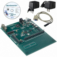
KIT DEV FOR ADUC824 QUICK START
Manufacturer
Analog Devices Inc
Series
QuickStart™ Kitr
Type
8052-corer
Datasheet
1.EVAL-ADUC824QSZ.pdf
(68 pages)
Specifications of EVAL-ADUC824QS
Contents
Evaluation Board, Power Supply, Cable, Software and Documentation
For Use With/related Products
ADuC824
Lead Free Status / RoHS Status
Contains lead / RoHS non-compliant


ADuC824
Three SFRs are used to control the I
Bit
7
6
5
4
3
2
1
0
I
The ADuC824 supports a 2-wire serial interface mode which is
I
with the on-chip SPI interface and therefore the user can only
enable one or the other interface at any given time (see SPE in
I2CADD
Function
SFR Address
Power-On Default Value
Bit Addressable
2
2
C-COMPATIBLE INTERFACE
C compatible. The I
SDATA (Pin 27)
SCLOCK (Pin 26)
I2CCON
SFR Address
Power-On Default Value
Bit Addressable
M
D
O
Name
MDO
MDE
MCO
MDI
I2CM
I2CRS
I2CTX
I2CI
M
2
C-compatible interface shares its pins
D
E
I
Holds the I
the part. It may be overwritten by
user code. Technical Note uC001 at
www.analog.com/microconverter
describes the format of the I
dard 7-bit address in detail.
9BH
55H
No
2
C Address Register
Serial Data I/O Pin
Serial Clock
2
I
E8H
00H
Yes
Description
I
This data bit is used to implement a master I
bit will be outputted on the SDATA pin if the data output enable (MDE) bit is set.
I
Set by user to enable the SDATA pin as an output (Tx).
Cleared by the user to enable SDATA pin as an input (Rx).
I
This data bit is used to implement a master I
this bit will be outputted on the SCLOCK pin.
I
This data bit is used to implement a master I
pin is latched into this bit on SCLOCK if the Data Output Enable (MDE) bit is ‘0.’
I
Set by user to enable I
Cleared by user to enable I
I
Set by user to reset the I
Cleared by user code for normal I
I
Set by the MicroConverter if the interface is transmitting.
Cleared by the MicroConverter if the interface is receiving.
I
Set by the MicroConverter after a byte has been transmitted or received.
Cleared automatically when user code reads the I2CDAT SFR (see I2CDAT below).
C-compatible interface. These are described below:
2
2
2
2
2
2
2
2
2
C Control Register
C Software Master Data Output Bit (MASTER MODE ONLY)
C Software Master Data Output Enable Bit (MASTER MODE ONLY)
C Software Master Clock Output Bit (MASTER MODE ONLY)
C Software Master Data Input Bit (MASTER MODE ONLY)
C Master/Slave Mode Bit
C Reset Bit (SLAVE MODE ONLY)
C Direction Transfer Bit (SLAVE MODE ONLY)
C Interrupt Bit (SLAVE MODE ONLY)
M
2
C peripheral address for
C
O
Table XX. I2CCON SFR Bit Designations
M
2
C stan-
D
2
C software master mode.
I
2
C interface.
2
C hardware slave mode.
SPICON previously). An Application Note describing the
operation of this interface as implemented is available from
the MicroConverter Website at
This interface can be configured as a Software Master or Hard-
ware Slave, and uses two pins in the interface.
I2CDAT
Function
SFR Address
Power-On Default Value
Bit Addressable
2
C operation.
2 I
C
M
2
C transmitter interface in software. Data written to this
2
C receiver interface in software. Data on the SDATA
2
C transmitter interface in software. Data written to
2 I
C
R
S
The I2CDAT SFR is written by the
I
user to transmit data over the I
interface or read by user code to read
data just received by the I
Accessing I2CDAT automatically
clears any pending I
the I2CI bit in the I2CCON SFR.
User software should only access
I2CDAT once per interrupt cycle.
9AH
00H
No
2
C Data Register
www.analog.com/microconverter.
2 I
C
T
X
2
C interrupt and
2
C interface
2 I
C
I
2
C
Related parts for EVAL-ADUC824QS
Image
Part Number
Description
Manufacturer
Datasheet
Request
R


Part Number:
Description:
BOARD EVAL FOR SI270X-A
Manufacturer:
Silicon Laboratories Inc
Datasheet:

Part Number:
Description:
BUCK CONV REF DESIGN KIT IP1201
Manufacturer:
International Rectifier
Datasheet:
Part Number:
Description:
BOARD DEMO SYNC DUAL BUCK CNVTER
Manufacturer:
International Rectifier
Datasheet:
Part Number:
Description:
BOARD DEMO SYNC BUCK CONVETER
Manufacturer:
International Rectifier
Datasheet:

Part Number:
Description:
EVALBOARD/EB Omnidirectional microphone - Analog
Manufacturer:
Analog Devices
Datasheet:
Part Number:
Description:
EVALBOARD/EB Omnidirectional microphone - Analog
Manufacturer:
Analog Devices
Datasheet:


Part Number:
Description:
BOARD EVAL LED DRIVER LT3756
Manufacturer:
Linear Technology
Datasheet:

Part Number:
Description:
BOARD EVAL FOR AD7741/7742
Manufacturer:
Analog Devices Inc
Datasheet:

Part Number:
Description:
±1.7g Dual-Axis IMEMS Accelerometer Evaluation Board
Manufacturer:
Analog Devices Inc
Datasheet:

Part Number:
Description:
IC MULTIPLIER ANALOG 8-SOIC T/R
Manufacturer:
Analog Devices Inc
Datasheet:

Part Number:
Description:
IC ANALOG MULTIPLIER 8-DIP
Manufacturer:
Analog Devices Inc
Datasheet:
Part Number:
Description:
IC ANALOG MULTIPLIER 8-SOIC
Manufacturer:
Analog Devices Inc
Datasheet:
Part Number:
Description:
IC ANALOG MULTIPLIER 8-DIP
Manufacturer:
Analog Devices Inc
Datasheet: