HDJD-JD05 Avago Technologies US Inc., HDJD-JD05 Datasheet - Page 11
HDJD-JD05
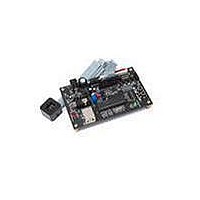
Manufacturer Part Number
HDJD-JD05
Description
KIT DEV RGB COLOR SENSOR 20-QFN
Manufacturer
Avago Technologies US Inc.
Specifications of HDJD-JD05
Sensor Type
Light, Color Sensor
Sensing Range
RGB
Interface
2-Wire Serial
Voltage - Supply
2.5 V ~ 3.6 V
Embedded
No
Utilized Ic / Part
ADJD-S313-QR999
For Use With/related Products
ADJD-S313-QR999
Lead Free Status / RoHS Status
Not applicable / Not applicable


Data format
ADJD-S313 uses a register-based programming
architecture. Each register has a unique address and
controls a specific function inside the chip.
To write to a register, the master first generates a
START condition. Then it sends the slave address
for the device it wants to communicate with. The
least significant bit (LSB) of the slave address must
indicate that the master wants to write to the slave.
The addressed device will then acknowledge the
master.
The master writes the register address it wants to
access and waits for the slave to acknowledge. The
master then writes the new register data. Once the
slave acknowledges, the master generates a STOP
condition to end the data transfer.
Figure 8. Register Byte Write Protocol
Start condition
Figure 9. Register Byte Read Protocol
Start condition
11
S
S
A6 A5 A4 A3 A2 A1 A0 W
A6 A5 A4 A3 A2 A1 A0 W
slave address
slave address
Master sends
Master sends
Master will write data
Master will write data
Slave acknowledge
Slave acknowledge
A
A
D7 D6 D5 D4 D3 D2 D1 D0
D7 D6 D5 D4 D3 D2 D1 D0
register address
register address
Master writes
Master writes
Slave acknowledge
Slave acknowledge
Repeated start
condition
A
A
D7 D6 D5 D4 D3 D2 D1 D0
Sr
A6 A5 A4 A3 A2 A1 A0 R
To read from a register, the master first generates
a START condition. Then it sends the slave address
for the device it wants to communicate with. The
least significant bit (LSB) of the slave address must
indicate that the master wants to write to the slave.
The addressed device will then acknowledge the
master.
The master writes the register address it wants to
access and waits for the slave to acknowledge. The
master then generates a repeated START condition
and resends the slave address sent previously. The
least significant bit (LSB) of the slave address must
indicate that the master wants to read from the
slave. The addressed device will then acknowledge
the master.
The master reads the register data sent by the slave
and sends a no acknowledge signal to stop reading.
The master then generates a STOP condition to end
the data transfer.
Master writes
register data
slave address
Master sends
Master will read data
Slave acknowledge
Slave acknowledge
Stop condition
A
P
A
D7 D6 D5 D4 D3 D2 D1 D0
Master reads
register data
acknowledge
Master not
Stop condition
A
P
Related parts for HDJD-JD05
Image
Part Number
Description
Manufacturer
Datasheet
Request
R

Part Number:
Description:
KIT DEV RGB COLOR SENSOR 16-QFN
Manufacturer:
Avago Technologies US Inc.
Datasheet:

Part Number:
Description:
KIT DEV RGB COLOR SENSOR 16-QFN
Manufacturer:
Avago Technologies US Inc.
Datasheet:

Part Number:
Description:
KIT DEV RGB DCS 2.2X2.2
Manufacturer:
Avago Technologies US Inc.
Datasheet:

Part Number:
Description:
Optical Sensor
Manufacturer:
Avago Technologies US Inc.
Datasheet:
Part Number:
Description:
RGB COLOR CONTROLLER AND SENSOR
Manufacturer:
Avago Technologies US Inc.
Part Number:
Description:
Photodiodes Color Controller
Manufacturer:
Avago Technologies US Inc.

Part Number:
Description:
Optical Sensors - Board Mount RGB Color Sensor
Manufacturer:
Avago Technologies US Inc.

Part Number:
Description:
Optical Sensors - Board Mount RGB Color Sensor
Manufacturer:
Avago Technologies US Inc.

Part Number:
Description:
Optical Sensor Development Tools RGB CONTROLLER Development Kit
Manufacturer:
Avago Technologies US Inc.

Part Number:
Description:
Optical Sensor Development Tools RGB CONTROLLER Development Kit
Manufacturer:
Avago Technologies US Inc.

Part Number:
Description:
OPTOCOUPLER GATE DRV 2A 16-SOIC
Manufacturer:
Avago Technologies US Inc.
Datasheet:
Part Number:
Description:
OPTOCOUPLER 2CH 2.5A 16-SOIC
Manufacturer:
Avago Technologies US Inc.
Datasheet:

Part Number:
Description:
OPTOCOUPLER GATE DRV 0.4A 16SOIC
Manufacturer:
Avago Technologies US Inc.
Datasheet:

Part Number:
Description:
OPTOCOUPLER 2.0A 250KHZ 8-DIP
Manufacturer:
Avago Technologies US Inc.
Datasheet:

Part Number:
Description:
OPTOCOUPLER 2.0A 250KHZ GW 8-SMD
Manufacturer:
Avago Technologies US Inc.
Datasheet: