RDK-160 Power Integrations, RDK-160 Datasheet - Page 13
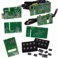
RDK-160
Manufacturer Part Number
RDK-160
Description
KIT REF DESIGN LINKSWITCH 2
Manufacturer
Power Integrations
Series
LinkSwitch-IIr
Type
MOSFET & Power Driverr
Datasheet
1.LNK603DG.pdf
(18 pages)
Specifications of RDK-160
Mfg Application Notes
LinkSwitch-II Family, Appl Note AN-44
Design Resources
RDR-157, 2.78W USB Charger Using LNK613DG RDR-158, 5W Charger Using LNK616PG RDR-159, 2.4W Charger Using LNK603DG
Main Purpose
AC/DC, Primary Side
Outputs And Type
1, Isolated
Voltage - Input
85 ~ 265VAC
Regulator Topology
Flyback
Board Type
Bare (Unpopulated) and Fully Populated
Utilized Ic / Part
LNK603, LNK604, LNK605, LNK606, LNK613, LNK614, LNK615, LNK616
Product
Power Management Modules
Lead Free Status / RoHS Status
Lead free by exemption / RoHS Compliant
For Use With/related Products
LNK60x, LNK61x
Other names
596-1235


Figure 19. Test Set-up for Feedback Pin Measurements.
Figure 20. Test Set-up for Leakage and Breakdown Tests.
www.powerint.com
1) Raise V
2) Raise V
3) Reduce V
4) Apply 1.5 V at V
BP
IN
until cycle skipping occurs at V
IN
voltage from 0 V to 6.2 V, down to 4.5 V, up to 6.2 V
5 µF
until cycle skipping stops at V
V
IN
IN
and measure t
+
To measure BV
1) Close S1, open S2
2) Power-up V
3) Open S1, close S2
4) Measure I/V characteristics of Drain pin using the curve tracer
50 kΩ
16 V
V
+
6.2 V
IN
+
10 kΩ
FB
4 kΩ
delay from start of cycle falling edge to the next falling edge
IN
10 µF
DSS
source (16 V)
, I
OUT
DSS1
OUT
LinkSwitch-II
to measure V
, and I
to measure V
FB
BP
D
1 µF
DSS2
S
S
S
S
follow these steps:
S1
FBth
FBth-
. Cable drop compensaion factor is υ
.1 µF
S2
LinkSwitch-II
BP
FB
D
Tracer
Curve
500 Ω
PI-4961-022708
S
S
S
S
V
OUT
+
LNK603-606/613-616
2 V
FB
= V
FBth
/ V
FBth-
PI-4962-040308
Rev. F 01/10
13
Related parts for RDK-160
Image
Part Number
Description
Manufacturer
Datasheet
Request
R

Part Number:
Description:
KIT REF DESIGN FOR LNK457D
Manufacturer:
Power Integrations
Datasheet:

Part Number:
Description:
REFERENCE DESIGN LINKSWITCH-PH
Manufacturer:
Power Integrations
Datasheet:

Part Number:
Description:
KIT REF DESIGN FOR LNK403EG
Manufacturer:
Power Integrations
Datasheet:

Part Number:
Description:
KIT REF DESIGN FOR LNK406EG
Manufacturer:
Power Integrations
Datasheet:

Part Number:
Description:
KIT REF DESIGN LINKSWITCH-CV
Manufacturer:
Power Integrations
Datasheet:

Part Number:
Description:
Specifications: Family: Eval Boards - DC/DC & AC/DC (Off-Line) SMPS ; Series: HiperLCS™ ; Main Purpose: DC/DC, Step Down ; Outputs and Type: 1, Isolated ; Power - Output: 150W ; Voltage - Output: 24V ; Current - Output: 6.25A ; Voltage - Input:
Manufacturer:
Power Integrations, Inc.
Datasheet:

Part Number:
Description:
KIT DESIGN REF TINYSWITCH-III
Manufacturer:
Power Integrations
Datasheet:

Part Number:
Description:
KIT DESIGN REF LINKSWITCH LP
Manufacturer:
Power Integrations
Datasheet:

Part Number:
Description:
KIT REF DESIGN LED LINKSWITCH TN
Manufacturer:
Power Integrations
Datasheet:
Part Number:
Description:
KIT REF DESIGN PG LINKSWITCH-II
Manufacturer:
Power Integrations
Datasheet:
Part Number:
Description:
REFERENCE DESIGN LINKSWITCH-PL
Manufacturer:
Power Integrations
Datasheet:
Part Number:
Description:
REFERENCE DESIGN LINKSWITCH-PH
Manufacturer:
Power Integrations
Datasheet:

Part Number:
Description:
KIT REF DESIGN 36-72W MOTOR DRVR
Manufacturer:
Power Integrations
Datasheet:
Part Number:
Description:
Specifications: Manufacturer: Power Integrations ; Output Voltage: 380 VDC ; Input / Supply Voltage (Max): 264 VAC ; Input / Supply Voltage (Min): 90 VAC ; Mounting Style: Through Hole ; Output Current: 0.913 A ; Output Power: 347 W
Manufacturer:
Power Integrations, Inc.

Part Number:
Description:
KIT REF DESIGN TOP HX FOR TOP258
Manufacturer:
Power Integrations
Datasheet: