RDK-160 Power Integrations, RDK-160 Datasheet - Page 2
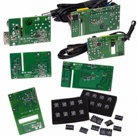
RDK-160
Manufacturer Part Number
RDK-160
Description
KIT REF DESIGN LINKSWITCH 2
Manufacturer
Power Integrations
Series
LinkSwitch-IIr
Type
MOSFET & Power Driverr
Datasheet
1.LNK603DG.pdf
(18 pages)
Specifications of RDK-160
Mfg Application Notes
LinkSwitch-II Family, Appl Note AN-44
Design Resources
RDR-157, 2.78W USB Charger Using LNK613DG RDR-158, 5W Charger Using LNK616PG RDR-159, 2.4W Charger Using LNK603DG
Main Purpose
AC/DC, Primary Side
Outputs And Type
1, Isolated
Voltage - Input
85 ~ 265VAC
Regulator Topology
Flyback
Board Type
Bare (Unpopulated) and Fully Populated
Utilized Ic / Part
LNK603, LNK604, LNK605, LNK606, LNK613, LNK614, LNK615, LNK616
Product
Power Management Modules
Lead Free Status / RoHS Status
Lead free by exemption / RoHS Compliant
For Use With/related Products
LNK60x, LNK61x
Other names
596-1235


Figure 2
Pin Functional Description
DRAIN (D) Pin:
This pin is the power MOSFET drain connection. It provides
internal operating current for both start-up and steady-state
operation.
BYPASS/MULTI-FUNCTIONAL PROGRAMMABLE
(BP/M) Pin:
This pin has multiple functions:
1. It is the connection point for an external bypass capacitor for
2. It is a mode selection for the cable drop compensation for
FEEDBACK (FB) Pin:
During normal operation, switching of the power MOSFET is
controlled by this pin. This pin senses the AC voltage on the bias
winding. This control input regulates both the output voltage in
CV mode and output current in CC mode based on the flyback
voltage of the bias winding. The internal inductance correction
circuit uses the forward voltage on the bias winding to sense the
bulk capacitor voltage.
SOURCE (S) Pin:
This pin is internally connected to the output MOSFET source for
high voltage power and control circuit common returns.
Rev. F 01/10
2
the internally generated 6 V supply.
LNK61X series.
FEEDBACK
SOURCE
BYPASS
LNK603-606/613-616
(BP/M)
(FB)
(S)
6.5 V
Functional Block Diagram.
COMPENSATION
V
CORRECTION
CABLE DROP
TH
INDUCTANCE
CONSTANT
CURRENT
t
SAMPLE-OUT
+
-
t
SAMPLE-INPUT
D
V
ILIMIT
FB
Q
DC
OUT
MAX
I
FB
LIM
I
LIM
DC
OSCILLATOR
Auto-Restart
MACHINE
Open-Loop
MAX
STATE
FAULT
Figure 3.
Drive
BP/M
Reset
FB
G Package (SMD-8C)
P Package (DIP-8C)
D
V
ILIMIT
SHUTDOWN
THERMAL
Pin Configuration.
1
2
4
Current Limit
Comparator
t
SAMPLE-INPUT
t
SAMPLE-OUT
6 V
5 V
+
-
3a
V
+
-
ILIMIT
8
7
6
5
SAMPLE
BLANKING
S
S
DELAY
S
S
LEADING
EDGE
REGULATOR
BP/M
D Package (SO-8C)
FB
D
6 V
1
2
4
www.powerint.com
3b
PI-3491-012808
PI-4908-041508
8
7
6
5
SOURCE
DRAIN
(D)
S
S
(S)
S
S
Related parts for RDK-160
Image
Part Number
Description
Manufacturer
Datasheet
Request
R

Part Number:
Description:
KIT REF DESIGN FOR LNK457D
Manufacturer:
Power Integrations
Datasheet:

Part Number:
Description:
REFERENCE DESIGN LINKSWITCH-PH
Manufacturer:
Power Integrations
Datasheet:

Part Number:
Description:
KIT REF DESIGN FOR LNK403EG
Manufacturer:
Power Integrations
Datasheet:

Part Number:
Description:
KIT REF DESIGN FOR LNK406EG
Manufacturer:
Power Integrations
Datasheet:

Part Number:
Description:
KIT REF DESIGN LINKSWITCH-CV
Manufacturer:
Power Integrations
Datasheet:

Part Number:
Description:
Specifications: Family: Eval Boards - DC/DC & AC/DC (Off-Line) SMPS ; Series: HiperLCS™ ; Main Purpose: DC/DC, Step Down ; Outputs and Type: 1, Isolated ; Power - Output: 150W ; Voltage - Output: 24V ; Current - Output: 6.25A ; Voltage - Input:
Manufacturer:
Power Integrations, Inc.
Datasheet:

Part Number:
Description:
KIT DESIGN REF TINYSWITCH-III
Manufacturer:
Power Integrations
Datasheet:

Part Number:
Description:
KIT DESIGN REF LINKSWITCH LP
Manufacturer:
Power Integrations
Datasheet:

Part Number:
Description:
KIT REF DESIGN LED LINKSWITCH TN
Manufacturer:
Power Integrations
Datasheet:
Part Number:
Description:
KIT REF DESIGN PG LINKSWITCH-II
Manufacturer:
Power Integrations
Datasheet:
Part Number:
Description:
REFERENCE DESIGN LINKSWITCH-PL
Manufacturer:
Power Integrations
Datasheet:
Part Number:
Description:
REFERENCE DESIGN LINKSWITCH-PH
Manufacturer:
Power Integrations
Datasheet:

Part Number:
Description:
KIT REF DESIGN 36-72W MOTOR DRVR
Manufacturer:
Power Integrations
Datasheet:
Part Number:
Description:
Specifications: Manufacturer: Power Integrations ; Output Voltage: 380 VDC ; Input / Supply Voltage (Max): 264 VAC ; Input / Supply Voltage (Min): 90 VAC ; Mounting Style: Through Hole ; Output Current: 0.913 A ; Output Power: 347 W
Manufacturer:
Power Integrations, Inc.

Part Number:
Description:
KIT REF DESIGN TOP HX FOR TOP258
Manufacturer:
Power Integrations
Datasheet: