752161473GPTR CTS Resistor Products, 752161473GPTR Datasheet - Page 12
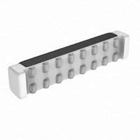
752161473GPTR
Manufacturer Part Number
752161473GPTR
Description
RES-NET 47K OHM BUSSED SMD
Manufacturer
CTS Resistor Products
Series
752r
Specifications of 752161473GPTR
Resistance (ohms)
47K
Number Of Resistors
14
Circuit Type
Bussed
Temperature Coefficient
±200ppm/°C
Tolerance
±2%
Power Per Element
80mW
Number Of Pins
16
Package / Case
16-DRT
Size / Dimension
0.465" L x 0.080" W (11.81mm x 2.03mm)
Height
0.095" (2.41mm)
Mounting Type
Surface Mount
Operating Temperature
-55°C ~ 125°C
Lead Free Status / RoHS Status
Lead free / RoHS Compliant
Other names
752-161-47KPTR


www.national.com
Application Information
nal power dissipation is 4 times that of a single-ended am-
plifier. The maximum power dissipation for a given BTL
application can be derived from Equation 1.
BOOST CONVERTER POWER DISSIPATION
At higher duty cycles, the increased ON-time of the switch
FET means the maximum output current will be determined
by power dissipation within the LM2731 FET switch. The
switch power dissipation from ON-time conduction is calcu-
lated by Equation 2.
where DC is the duty cycle.
There will be some switching losses as well, so some derat-
ing needs to be applied when calculating IC power dissipa-
tion.
TOTAL POWER DISSIPATION
The total power dissipation for the LM4805 can be calculated
by adding Equation 1 and Equation 2 together to establish
Equation 3:
The result from Equation 3 must not be greater than the
power dissipation that results from Equation 4:
For the LQA28A, θ
LM4805. Depending on the ambient temperature, T
system surroundings, Equation 4 can be used to find the
maximum internal power dissipation supported by the IC
packaging. If the result of Equation 3 is greater than that of
Equation 4, then either the supply voltage must be in-
creased, the load impedance increased or T
the typical application of a 3V power supply, with V1 set to
5.5V and an 8Ω load, the maximum ambient temperature
possible without violating the maximum junction temperature
is approximately 111˚C provided that device operation is
around the maximum power dissipation point. Thus, for typi-
cal applications, power dissipation is not an issue. Power
dissipation is a function of output power and thus, if typical
operation is not around the maximum power dissipation
point, the ambient temperature may be increased accord-
ingly. Refer to the Typical Performance Characteristics
curves for power dissipation information for lower output
levels.
EXPOSED-DAP PACKAGE PCB MOUNTING
CONSIDERATIONS
The LM4805’s exposed-DAP (die attach paddle) package
(LD) provides a low thermal resistance between the die and
the PCB to which the part is mounted and soldered. The low
thermal resistance allows rapid heat transfer from the die to
the surrounding PCB copper traces, ground plane, and sur-
rounding air. The LD package should have its DAP soldered
to a copper pad on the PCB. The DAP’s PCB copper pad
P
DMAX(TOTAL)
P
DMAX(SWITCH)
P
DMAX(AMP)
P
DMAX
= [4*(V
JA
= DC x I
= (T
= 59˚C/W. T
x R
DD
= 4(V
)
DS
JMAX
2
/2π
(ON)]
IND
DD
2
- T
R
(AVE)
)
L
2
] + [DC x I
A
/ (2π
) / θJA
JMAX
2
2
x R
(Continued)
R
= 125˚C for the
L
A
)
DS
IND
reduced. For
(ON)
(AVE)
A
, of the
2
(1)
(2)
(3)
(4)
12
may be connected to a large plane of continuous unbroken
copper. This plane forms a thermal mass, heat sink, and
radiation area. Further detailed and specific information con-
cerning PCB layout, fabrication, and mounting an LD (LLP)
package is found in National Semiconductor’s Package En-
gineering Group under application note AN1187.
SHUTDOWN FUNCTION
In many applications, a microcontroller or microprocessor
output is used to control the shutdown circuitry to provide a
quick, smooth transition into shutdown. Another solution is to
use a single-pole, single-throw switch, and a pull-up resistor.
One terminal of the switch is connected to GND. The other
side is connected to the two shutdown pins and the terminal
of the pull-up resistor. The remaining resistance terminal is
connected to V
pull-up resistor connected to V
This scheme guarantees that the shutdown pins will not float
thus preventing unwanted state changes.
PROPER SELECTION OF EXTERNAL COMPONENTS
Proper selection of external components in applications us-
ing integrated power amplifiers, and switching boost convert-
ers, is critical for optimizing device and system performance.
Consideration to component values must be used to maxi-
mize overall system quality.
The best capacitors for use with the switching converter
portion of the LM4805 are multi-layer ceramic capacitors.
They have the lowest ESR (equivalent series resistance)
and highest resonance frequency, which makes them opti-
mum for high frequency switching converters.
When selecting a ceramic capacitor, only X5R and X7R
dielectric types should be used. Other types such as Z5U
and Y5F have such severe loss of capacitance due to effects
of temperature variation and applied voltage, they may pro-
vide as little as 20% of rated capacitance in many typical
applications. Always consult capacitor manufacturer’s data
curves before selecting a capacitor. High-quality ceramic
capacitors can be obtained from Taiyo-Yuden, AVX, and
Murata.
POWER SUPPLY BYPASSING
As with any amplifier, proper supply bypassing is critical for
low noise performance and high power supply rejection. The
capacitor location on both V1 and V
should be as close to the device as possible.
SELECTING INPUT CAPACITOR FOR AUDIO
AMPLIFIER
One of the major considerations is the closedloop bandwidth
of the amplifier. To a large extent, the bandwidth is dictated
by the choice of external components shown in Figure 1. The
input coupling capacitor, C
which limits low frequency response. This value should be
chosen based on needed frequency response for a few
distinct reasons.
High value input capacitors are both expensive and space
hungry in portable designs. Clearly, a certain value capacitor
is needed to couple in low frequencies without severe at-
tenuation. However, speakers used in portable systems,
whether internal or external, have little ability to reproduce
signals below 100Hz to 150Hz. Thus, using a high value
input capacitor may not increase actual system perfor-
mance.
In addition to system cost and size, click and pop perfor-
mance is affected by the value of the input coupling capaci-
DD
. If the switch is open, then the external
i
, forms a first order high pass filter
DD
will enable the LM4805.
DD
(Cs2 and Cs1) pins
Related parts for 752161473GPTR
Image
Part Number
Description
Manufacturer
Datasheet
Request
R

Part Number:
Description:
RESISTOR NET 4.7K OHM SMD
Manufacturer:
CTS Resistor Products
Datasheet:

Part Number:
Description:
RES .10 OHM 1/8W 5% 0805
Manufacturer:
CTS Resistor Products
Datasheet:

Part Number:
Description:
RES .20 OHM 1/10W 5% 0402
Manufacturer:
CTS Resistor Products
Datasheet:

Part Number:
Description:
RES .47 OHM 1/8W 5% 0805
Manufacturer:
CTS Resistor Products
Datasheet:

Part Number:
Description:
RES .47 OHM 1/10W 5% 0402
Manufacturer:
CTS Resistor Products
Datasheet:

Part Number:
Description:
RES .47 OHM 1/4W 5% 1206
Manufacturer:
CTS Resistor Products
Datasheet:

Part Number:
Description:
RES .20 OHM 1/10W 5% 0603
Manufacturer:
CTS Resistor Products
Datasheet:

Part Number:
Description:
RES .47 OHM 1/2W 5% 1210
Manufacturer:
CTS Resistor Products
Datasheet:

Part Number:
Description:
RES .20 OHM 1/2W 5% 1210
Manufacturer:
CTS Resistor Products
Datasheet:

Part Number:
Description:
RES .47 OHM .75W 5% 2010
Manufacturer:
CTS Resistor Products
Datasheet:

Part Number:
Description:
RES .20 OHM .75W 5% 2010
Manufacturer:
CTS Resistor Products
Datasheet:

Part Number:
Description:
RES .56 OHM .75W 5% 2010
Manufacturer:
CTS Resistor Products
Datasheet:

Part Number:
Description:
RES .91 OHM .75W 5% 2010
Manufacturer:
CTS Resistor Products
Datasheet:

Part Number:
Description:
RES .050 OHM .5W 5% 1206
Manufacturer:
CTS Resistor Products
Datasheet:

Part Number:
Description:
RES NET 15RES 4.7K OHM 16PIN SMD
Manufacturer:
CTS Resistor Products
Datasheet: