752161473GPTR CTS Resistor Products, 752161473GPTR Datasheet - Page 13
752161473GPTR
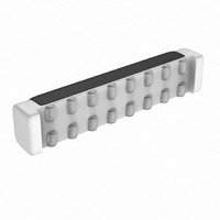
Manufacturer Part Number
752161473GPTR
Description
RES-NET 47K OHM BUSSED SMD
Manufacturer
CTS Resistor Products
Series
752r
Specifications of 752161473GPTR
Resistance (ohms)
47K
Number Of Resistors
14
Circuit Type
Bussed
Temperature Coefficient
±200ppm/°C
Tolerance
±2%
Power Per Element
80mW
Number Of Pins
16
Package / Case
16-DRT
Size / Dimension
0.465" L x 0.080" W (11.81mm x 2.03mm)
Height
0.095" (2.41mm)
Mounting Type
Surface Mount
Operating Temperature
-55°C ~ 125°C
Lead Free Status / RoHS Status
Lead free / RoHS Compliant
Other names
752-161-47KPTR


Application Information
tor, C
charge to reach its quiescent DC voltage (nominally 1/2
V
and is apt to create pops upon device enable. Thus, by
minimizing the capacitor value based on desired low fre-
quency response, turn-on pops can be minimized.
SELECTING BYPASS CAPACITOR FOR AUDIO
AMPLIFIER
Besides minimizing the input capacitor value, careful consid-
eration should be paid to the bypass capacitor value. Bypass
capacitor, C
turn-on pops since it determines how fast the amplifier turns
on. The slower the amplifier’s outputs ramp to their quies-
cent DC voltage (nominally 1/2 V
pop. Choosing C
C
virtually clickless and popless shutdown function. Although
the device will function properly, (no oscillations or motor-
boating), with C
more susceptible to turn-on clicks and pops. Thus, a value of
C
sensitive designs.
SELECTING FEEDBACK CAPACITOR FOR AUDIO
AMPLIFIER
The LM4805 is unity-gain stable which gives the designer
maximum system flexability. However, a typical application
requires a closed-loop differential gain of 10. In this case a
feedback capacitor (C
to bandwidth limit the amplifier.
This feedback capacitor creates a low pass filter that elimi-
nates possible high frequency oscillations. Care should be
taken when calculating the -3dB frequency because an in-
correct combination of R
desired frequency
SELECTING OUTPUT CAPACITOR (C
CONVERTER
A single 4.7µF to 10µF ceramic capacitor will provide suffi-
cient output capacitance for most applications. If larger
amounts of capacitance are desired for improved line sup-
port and transient response, tantalum capacitors can be
used. Aluminum electrolytics with ultra low ESR such as
Sanyo Oscon can be used, but are usually prohibitively
expensive. Typical AI electrolytic capacitors are not suitable
for switching frequencies above 500 kHz because of signifi-
cant ringing and temperature rise due to self-heating from
ripple current. An output capacitor with excessive ESR can
also reduce phase margin and cause instability.
In general, if electrolytics are used, we recommended that
they be paralleled with ceramic capacitors to reduce ringing,
switching losses, and output voltage ripple.
SELECTING INPUT CAPACITOR (Cs1) FOR BOOST
CONVERTER
An input capacitor is required to serve as an energy reservoir
for the current which must flow into the coil each time the
switch turns ON. This capacitor must have extremely low
ESR, so ceramic is the best choice. We recommend a
nominal value of 4.7µF, but larger values can be used. Since
this capacitor reduces the amount of voltage ripple seen at
the input pin, it also reduces the amount of EMI passed back
along that line to other circuitry.
DD
i
B
(in the range of 0.039µF to 0.39µF), should produce a
equal to 1.0µF is recommended in all but the most cost
). This charge comes from the output via the feedback
i
. A high value input coupling capacitor requires more
B
, is the most critical component to minimize
B
B
equal to 1.0µF along with a small value of
equal to 0.1µF, the device will be much
f
2) can be used as shown in Figure 2
f
and C
f
2 will cause rolloff before the
DD
), the smaller the turn-on
O
) FOR BOOST
(Continued)
13
SETTING THE OUTPUT VOLTAGE (V
CONVERTER
The output voltage is set using the external resistors R1 and
R2 (see Figure 1). A value of approximately 15k is recom-
mended for R2 to establish a divider current of approxi-
mately 92µA. R1 is calculated using the formula:
FEED-FORWARD COMPENSATION FOR BOOST
CONVERTER
Although the LM4805’s internal Boost converter is internally
compensated, the external feed-forward capacitor C
required for stability (see Figure 1). Adding this capacitor
puts a zero in the loop response of the converter. The
recommended frequency for the zero fz should be approxi-
mately 6kHz. C
SELECTING DIODES
The external diode used in Figure 1 should be a Schottky
diode. A 20V diode such as the MBR0520 is recommended.
The MBR05XX series of diodes are designed to handle a
maximum average current of 0.5A. For applications exceed-
ing 0.5A average but less than 1A, a Microsemi UPS5817
can be used.
DUTY CYCLE
The maximum duty cycle of the boost converter determines
the maximum boost ratio of output-to-input voltage that the
converter can attain in continuous mode of operation. The
duty cycle for a given boost application is defined as:
This applies for continuous mode operation.
INDUCTANCE VALUE
The first question we are usually asked is: “How small can I
make the inductor.” (because they are the largest sized
component and usually the most costly). The answer is not
simple and involves trade-offs in performance. Larger induc-
tors mean less inductor ripple current, which typically means
less output voltage ripple (for a given size of output capaci-
tor). Larger inductors also mean more load power can be
delivered because the energy stored during each switching
cycle is:
Where “lp” is the peak inductor current. An important point to
observe is that the LM4805 will limit its switch current based
on peak current. This means that since lp(max) is fixed,
increasing L will increase the maximum amount of power
available to the load. Conversely, using too little inductance
may limit the amount of load current which can be drawn
from the output.
Best performance is usually obtained when the converter is
operated in “continuous” mode at the load current range of
interest, typically giving better load regulation and less out-
Duty Cycle = V
f
1 can be calculated using the formula:
OUT
R1 = R2 X (V
C
f
1 = 1 / (2 X R1 X fz)
+ V
E = L/2 X (lp)2
DIODE
1
- V
/1.23 − 1)
IN
/ V
1
OUT
) OF BOOST
+ V
DIODE
www.national.com
- V
f
1 is
SW
(5)
(6)
Related parts for 752161473GPTR
Image
Part Number
Description
Manufacturer
Datasheet
Request
R

Part Number:
Description:
RESISTOR NET 4.7K OHM SMD
Manufacturer:
CTS Resistor Products
Datasheet:

Part Number:
Description:
RES .10 OHM 1/8W 5% 0805
Manufacturer:
CTS Resistor Products
Datasheet:

Part Number:
Description:
RES .20 OHM 1/10W 5% 0402
Manufacturer:
CTS Resistor Products
Datasheet:

Part Number:
Description:
RES .47 OHM 1/8W 5% 0805
Manufacturer:
CTS Resistor Products
Datasheet:

Part Number:
Description:
RES .47 OHM 1/10W 5% 0402
Manufacturer:
CTS Resistor Products
Datasheet:

Part Number:
Description:
RES .47 OHM 1/4W 5% 1206
Manufacturer:
CTS Resistor Products
Datasheet:

Part Number:
Description:
RES .20 OHM 1/10W 5% 0603
Manufacturer:
CTS Resistor Products
Datasheet:

Part Number:
Description:
RES .47 OHM 1/2W 5% 1210
Manufacturer:
CTS Resistor Products
Datasheet:

Part Number:
Description:
RES .20 OHM 1/2W 5% 1210
Manufacturer:
CTS Resistor Products
Datasheet:

Part Number:
Description:
RES .47 OHM .75W 5% 2010
Manufacturer:
CTS Resistor Products
Datasheet:

Part Number:
Description:
RES .20 OHM .75W 5% 2010
Manufacturer:
CTS Resistor Products
Datasheet:

Part Number:
Description:
RES .56 OHM .75W 5% 2010
Manufacturer:
CTS Resistor Products
Datasheet:

Part Number:
Description:
RES .91 OHM .75W 5% 2010
Manufacturer:
CTS Resistor Products
Datasheet:

Part Number:
Description:
RES .050 OHM .5W 5% 1206
Manufacturer:
CTS Resistor Products
Datasheet:

Part Number:
Description:
RES NET 15RES 4.7K OHM 16PIN SMD
Manufacturer:
CTS Resistor Products
Datasheet: