05045C103MA79A AVX Corporation, 05045C103MA79A Datasheet
05045C103MA79A
Specifications of 05045C103MA79A


Related parts for 05045C103MA79A

05045C103MA79A Summary of contents
Page 1
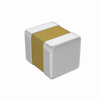
... AVX Multilayer Ceramic Chip Capacitor ...
Page 2
... Ceramic Chip Capacitors Table of Contents MLC Chip Capacitors General Description How to Order - AVX Part Number Explanation C0G (NP0) Dielectric General Specifications Typical Characteristic Curves Capacitance Range X7R Dielectric General Specifications Typical Characteristic Curves Capacitance Range Z5U Dielectric General Specifications Typical Characteristic Curves ...
Page 3
... General Description Basic Construction – A multilayer ceramic (MLC) capaci- tor is a monolithic block of ceramic containing two sets of offset, interleaved planar electrodes that extend to two opposite surfaces of the ceramic dielectric. This simple Ceramic Layer Formulations – Multilayer ceramic capacitors are available in both Class 1 and Class 2 formulations. Temperature ...
Page 4
... A typical curve of aging rate for semi- stable ceramics is shown in Figure Class 2 ceramic capacitor that has been sitting on the Curve 1 shelf for a period of time, is heated above its curie point, (125°C for 4 hours or 150°C for 2 ...
Page 5
... As a general statement, the piezoelectric output is higher, the higher the dielectric constant of the ceramic desirable to investigate this effect before using high “K” dielectrics as coupling capaci- tors in extremely low level applications. ...
Page 6
... Watts loss = (2 π fCV Very low values of dissipation factor are expressed as their reciprocal for convenience. These are called the “Q” Quality factor of capacitors. 2 π fC Parasitic Inductance – The parasitic inductance of capac- itors is becoming more and more important in the decou- pling of today’s high speed digital systems. The relationship ...
Page 7
... Another important, often overlooked, reason for knowing the parasitic inductance is the calculation of the resonant frequency. This can be important for high frequency, by- pass capacitors, as the resonant point will give the most signal attenuation. The resonant frequency is calculated from the simple equation: f ...
Page 8
... XI. Equivalent Series Resistance (ohms) XII. Power Loss (watts) XIII. KVA (Kilowatts) XIV. Temperature Characteristic (ppm/°C) XV. Cap Drift (%) XVI. Reliability of Ceramic Capacitors XVII. Capacitors in Series (current the same) XVIII. Capacitors in Parallel (voltage the same) XIX. Aging Rate (phase angle) XX. Decibels ...
Page 9
How to Order Part Number Explanation EXAMPLE: 08055A101JAT2A 0805 5 A Size Dielectric (L" x W") C0G (NP0 0402 X7R = C 0504 X5R = D 0603 Z5U = E 0805 Y5V = G 1005 0907 1206 1210 ...
Page 10
... Capacitance change with temperature is 0 ±30ppm/°C which is less than ±0.3% ∆ C from -55°C to +125°C. Capacitance drift or hysteresis for NP0 ceramics is negligible at less than ±0.05% versus up to ±2% for films. Typical capacitance change with life is less than ±0.1% for NP0s, one-fifth that shown by most other dielectrics ...
Page 11
... Variation of Impedance with Chip Size Impedance vs. Frequency 1000 pF - NP0 10 1206 0805 1812 1210 1.0 0.1 10 100 1000 Frequency, MHz Variation of Impedance with Ceramic Formulation Impedance vs. Frequency 1000 pF - NP0 vs X7R 0805 10.00 X7R NPO 1.00 0.10 0.01 10 100 1000 Frequency, MHz 100V 200V — ...
Page 12
C0G (NP0) Dielectric Capacitance Range SIZE 0402* MM 1.00 ± .10 (L) Length (in.) (.040 ± .004) MM .50 ± .10 (W) Width (in.) (.020 ± .004) (T) Max. Thickness MM .60 (in.) (.024) MM .25 ± .15 (t) Terminal ...
Page 13
C0G (NP0) Dielectric Capacitance Range SIZE 1210 MM 3.20 ± .20 (L) Length (in.) (.126 ± .008) MM 2.50 ± .20 (W) Width (in.) (.098 ± .008) MM 1.70 (T) Max. Thickness (in.) (.067) MM .50 ± .25 (t) Terminal ...
Page 14
... Dielectric Strength Test Voltage Test Frequency 12 X7R formulations are called “temperature-stable” ceramics and fall into EIA Class II materials. X7R is the most popular of these intermediate dielectric-constant materials. Its temperature variation of capacitance is with- in ±15% from -55°C to +125°C. This capacitance change is non-linear. ...
Page 15
X7R Dielectric Typical Characteristic Curves** Temperature Coefficient + -12 -18 -24 -75 -50 -25 0 +25 +50 +75 +100 +125 Temperature C Capacitance vs. Frequency +20 +10 0 -10 -20 1KHz 10 KHz 100 KHz Frequency Insulation ...
Page 16
X7R Dielectric Capacitance Range SIZE 0402* MM 1.00 ± .10 (L) Length (in.) (.040 ± .004) MM .50 ± .10 (W) Width (in.) (.020 ± .004) (T) Max. Thickness MM .60 (in.) (.024) MM .25 ± .15 (t) Terminal (in.) ...
Page 17
X7R Dielectric Capacitance Range SIZE 1210 MM 3.20 ± .20 (L) Length (in.) (.126 ± .008) MM 2.50 ± .20 (W) Width (in.) (.098 ± .008) MM 1.70 (T) Max. Thickness (in.) (.067) MM .50 ± .25 (t) Terminal (in.) ...
Page 18
... They provide the highest capacitance possible in a given size for the three most popular ceramic formulations. They show wide varia- tions in capacitance under influence of environmental and electrical operating conditions. Their aging rate is approxi- mately 5% per decade or 25% drop in ten years ...
Page 19
... Standard Sizes **For additional information on performance changes with operating conditions consult AVX’s software SpiCap. +50 +55 +65 +85 1 MHz 10 MHz Variation of Impedance with Ceramic Formulation +60 +70 +80 25V .01µF - .047µF .01µF - .12µF .01µF - .33µF .01µF - .56µF .01µF - .56µF .01µ ...
Page 20
Z5U Dielectric Capacitance Range SIZE MM (L) Length (in.) MM (W) Width (in.) MM (T) Max. Thickness (in.) MM (t) Terminal (in.) WVDC Cap .010 (µF) .012 .015 .018 .022 .027 .033 .039 .047 .056 .068 .082 .10 .12 .15 ...
Page 21
Z5U Dielectric Capacitance Range SIZE MM (L) Length (in.) MM (W) Width (in.) MM (T) Max. Thickness (in.) MM (t) Terminal (in.) WVDC Cap .010 (µF) .012 .015 .018 .022 .027 .033 .039 .047 .056 .068 .082 .10 .12 .15 ...
Page 22
Y5V Dielectric General Specifications PART NUMBER (see page 7 for complete information and options) 0805 3 G Size Voltage Dielectric (L" x W") 10V = Z Y5V = G 16V = Y 25V = 3 50V = 5 PERFORMANCE CHARACTERISTICS ...
Page 23
Y5V Dielectric Typical Characteristic Curves** Temperature Coefficient +20 +10 0 -10 -20 -30 -40 -50 -60 -70 -80 -55 -35 -15 +5 +25 +45 +65 +85 +105 +125 Temperature C Capacitance Change vs. DC Bias Voltage +40 +20 0 -20 ...
Page 24
Y5V Dielectric Capacitance Range SIZE 0402* 0603* MM 1.00 ± .10 1.60 ± .15 (L) Length (in.) (.040 ± .004) (.063 ± .006) MM .50 ± .10 .81 ± .15 (W) Width (in.) (.020 ± .004) (.032 ± .006) MM ...
Page 25
Low Profile Chips Z5U & Y5V Dielectric PART NUMBER (see page 7 for complete information and options) 1206 3 E Size Voltage Dielectric (L" x W") 25V = 3 Z5U = E Y5V = G PERFORMANCE CHARACTERISTICS Capacitance Range Capacitance ...
Page 26
... K 24 High value, low leakage and small size are difficult para- meters to obtain in capacitors for high voltage systems. AVX special high voltage MLC chips capacitors meet these performance characteristics and are designed for applica- tions such as snubbers in high frequency power converters, resonators in SMPS, and high voltage coupling/DC block- ing ...
Page 27
High Voltage Chips For 500V to 5000V Applications NP0 Dielectric PERFORMANCE CHARACTERISTICS Capacitance Range Capacitance Tolerances Dissipation Factor Operating Temperature Range Temperature Characteristic Voltage Ratings Insulation Resistance (+25°C, at 500 VDC) Insulation Resistance (+125°C, at 500 VDC) Dielectric Strength Thickness ...
Page 28
General Specifications Mechanical END TERMINATION ADHERENCE Specification No evidence of peeling of end terminal Measuring Conditions After soldering devices to circuit board apply 5N (0.51kg f) for 10 ± 1 seconds, please refer to Figure 1. 5N FORCE DEVICE UNDER ...
Page 29
General Specifications Environmental THERMAL SHOCK Specification Appearance No visual defects Capacitance Variation NP0: ± 2.5% or ± .25pF, whichever is greater X7R: ≤ ± 7.5% Z5U: ≤ ± 20% Y5V: ≤ ± 20% Q, Tan Delta To meet initial requirement ...
Page 30
General Specifications Environmental STEADY STATE HUMIDITY (No Load) Specification Appearance No visual defects Capacitance Variation NP0: ± ± .5pF, whichever is greater X7R: ≤ ± 10% Z5U: ≤ ± 30% Y5V: ≤ ± 30% Q, Tan Delta .......................Q ...
Page 31
MIL-C-55681/Chips Part Number Example W T MIL Style: CDR01, CDR02, CDR03, CDR04, CDR05, CDR06 Voltage Temperature Limits ± 30 ppm/°C without voltage; 0 ± 30 ppm/°C with rated voltage from -55°C to +125° ± 15% ...
Page 32
MIL-C-55681/Chips Military Part Number Identification CDR01 thru CDR06 Military Type Capacitance Capacitance Designation in pF tolerance AVX Style 0805/CDR01 CDR01BP100B--- 10 J,K CDR01BP120B--- 12 J CDR01BP150B--- 15 J,K CDR01BP180B--- 18 J CDR01BP220B--- 22 J,K CDR01BP270B--- 27 J CDR01BP330B--- 33 J,K ...
Page 33
MIL-C-55681/Chips Military Part Number Identification CDR31 thru CDR35 W T MIL Style: CDR31, CDR32, CDR33, CDR34, CDR35 Voltage Temperature Limits ± 30 ppm/°C without voltage; 0 ± 30 ppm/°C with rated voltage from -55°C to +125°C BX ...
Page 34
MIL-C-55681/Chips Military Part Number Identification CDR31 Military Type Capacitance Capacitance Designation tolerance AVX Style 0805/CDR31 (BP) CDR31BP1R0B--- 1.0 C CDR31BP1R1B--- 1.1 C CDR31BP1R2B--- 1.2 C CDR31BP1R3B--- 1.3 C CDR31BP1R5B--- 1.5 C CDR31BP1R6B--- 1.6 C CDR31BP1R8B--- 1.8 ...
Page 35
MIL-C-55681/Chips Military Part Number Identification CDR32 Military Type Capacitance Capacitance Designation tolerance AVX Style 1206/CDR32 (BP) CDR32BP1R0B--- 1.0 C CDR32BP1R1B--- 1.1 C CDR32BP1R2B--- 1.2 C CDR32BP1R3B--- 1.3 C CDR32BP1R5B--- 1.5 C CDR32BP1R6B--- 1.6 C CDR32BP1R8B--- 1.8 ...
Page 36
MIL-C-55681/Chips Military Part Number Identification CDR33/34/35 Military Type Capacitance Capacitance Designation tolerance AVX Style 1210/CDR33 (BP) CDR33BP102B--- 1,000 F,J,K CDR33BP112B--- 1,100 F,J,K CDR33BP122B--- 1,200 F,J,K CDR33BP132B--- 1,300 F,J,K CDR33BP152B--- 1,500 F,J,K CDR33BP162B--- 1,600 F,J,K CDR33BP182B--- 1,800 ...
Page 37
... European Detail Specification CECC 32 101-801/Chips Standard European Ceramic Chip Capacitors PART NUMBER (example) 0805 5 C Size Voltage Dielectric (L" x W") 50V = 100V = 1 2R1 = C 200V = 2 2F4 = G RANGE OF APPROVED COMPONENTS Case Dielectric Size Type 1BCG 0603 1B CG 0805 1B CG 1206 1B CG 1210 1B CG ...
Page 38
Packaging of Chip Components Automatic Insertion Packaging TAPE & REEL QUANTITIES All tape and reel specifications are in compliance with RS481. Embossed or Punched Carrier Embossed Only Punched Only Qty. per Reel/7" Reel Qty. per Reel/13" Reel (1) Dependent on ...
Page 39
Embossed Carrier Configuration 8 & Tape Only 8 & Embossed Tape Metric Dimensions Will Govern CONSTANT DIMENSIONS Tape Size +0.10 8mm 8.4 1.75 ± 0.10 -0.0 +.004 (.059 ) (.069 ± .004) (.157 ...
Page 40
Punched Carrier Configuration 8 & Tape Only 8 & Punched Tape Metric Dimensions Will Govern CONSTANT DIMENSIONS Tape Size +0.1 8mm 1.5 1.75 ± 0.10 -0.0 (.059 +.004 ) (.069 ± .004) and ...
Page 41
Bulk Case Packaging BENEFITS • Easier handling • Smaller packaging volume (1/20 of T/R packaging) • Easier inventory control • Flexibility • Recyclable CASE DIMENSIONS Shutter Slider 12mm 36mm 110mm Attachment Base CASE QUANTITIES Part Size Qty. (pcs / cassette) ...
Page 42
... Copper Copper c 1 Invar Filled Epoxy FR4/G10 Solder Fillet Nickel Polyimide/Glass Polyimide/Kevlar Silver Steel Tantalum Tin/Lead Ceramic CTE 9.5 to 11.5 ppm /o c Maximum Stress 4 Solder Fillet Electrodes CTE 18ppm /o c 140 W mK CTE and Conductivity of MLC Materials. 5W/m Kelvin 380W/m Kelvin 140W/m Kelvin CTE (ppm/° ...
Page 43
... Ceramic chips can easily be damaged and contaminated by poor handling or storage. A chip or crack, contamination by hands or poor storage, use of metal tweezers (the surface or bare ceramic chips is very abrasive) can all induce subse- quent defect as described above. Care must be taken to achieve the best results. ...
Page 44
... Component pads should be designed to achieve good sol- der filets and minimize component movement during reflow soldering. Pad designs are given below for the most com- mon sizes of multilayer ceramic capacitors for both wave and reflow soldering. The basis of these designs is: • Pad width equal to component width permissible to decrease this to as low as 85% of component width but it is not advisable to go below this ...
Page 45
... For further specific application or process advice please consult AVX. Cleaning Care should be taken to ensure that the capacitors are thoroughly cleaned of flux residues especially the space beneath the capacitor. Such residues may otherwise become conductive and effectively offer a low resistance bypass to the capacitor ...
Page 46
... Specifications are typical and may not apply to all applications. 44 SpiCap (for MLC chip capacitors) SpiTan (for tantalum capacitors) SpiCalci (for power supply capacitors) SpiMic (for RF-Microwave capacitors) AVX/Elco representative ...
Page 47
NOTICE: Specifications are subject to change without notice. Contact your nearest AVX Sales Office for the latest specifications. All statements, information and data given herein are believed to be accurate and reliable, but are presented without guarantee, warranty, or responsibility ...
Page 48
USA AVX Myrtle Beach, SC Corporate Offices Tel: 843-448-9411 FAX: 843-448-1943 AVX Northwest, WA Tel: 360-669-8746 FAX: 360-699-8751 AVX North Central, IN Tel: 317-848-7153 FAX: 317-844-9314 AVX Northeast, MA Tel: 508-485-8114 FAX: 508-485-8471 AVX Mid-Pacific, CA Tel: 408-436-5400 FAX: 408-437-1500 ...