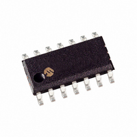
PIC16F616-I/SL Microchip Technology, PIC16F616-I/SL Datasheet - Page 73

PIC16F616-I/SL
Manufacturer Part Number
PIC16F616-I/SL
Description
IC PIC MCU FLASH 2KX14 14SOIC
Manufacturer
Microchip Technology
Series
PIC® 16Fr
Datasheets
1.PIC12F609T-ISN.pdf
(26 pages)
2.PIC16F616T-ISL.pdf
(4 pages)
3.PIC16F616T-ISL.pdf
(214 pages)
4.PIC16F616T-ISL.pdf
(8 pages)
5.PIC16F616-ESL.pdf
(180 pages)
Specifications of PIC16F616-I/SL
Program Memory Type
FLASH
Program Memory Size
3.5KB (2K x 14)
Package / Case
14-SOIC (3.9mm Width), 14-SOL
Core Processor
PIC
Core Size
8-Bit
Speed
20MHz
Peripherals
Brown-out Detect/Reset, POR, PWM, WDT
Number Of I /o
11
Ram Size
128 x 8
Voltage - Supply (vcc/vdd)
2 V ~ 5.5 V
Data Converters
A/D 8x10b
Oscillator Type
Internal
Operating Temperature
-40°C ~ 85°C
Processor Series
PIC16F
Core
PIC
Data Bus Width
8 bit
Data Ram Size
128 B
Maximum Clock Frequency
20 MHz
Number Of Programmable I/os
11
Number Of Timers
3
Maximum Operating Temperature
+ 85 C
Mounting Style
SMD/SMT
3rd Party Development Tools
52715-96, 52716-328, 52717-734
Development Tools By Supplier
PG164130, DV164035, DV244005, DV164005, PG164120, ICE2000
Minimum Operating Temperature
- 40 C
On-chip Adc
10 bit, 8 Channel
Lead Free Status / RoHS Status
Lead free / RoHS Compliant
For Use With
MCP1631RD-DCPC1 - REF DES BATT CHARG OR LED DRIVERAC162083 - HEADER MPLAB ICD2 PIC16F616 8/14
Eeprom Size
-
Connectivity
-
Lead Free Status / Rohs Status
Lead free / RoHS Compliant
Available stocks
Company
Part Number
Manufacturer
Quantity
Price
Company:
Part Number:
PIC16F616-I/SL
Manufacturer:
MICROCHIP
Quantity:
400
Company:
Part Number:
PIC16F616-I/SL
Manufacturer:
Microchip Technology
Quantity:
45 197
Part Number:
PIC16F616-I/SL
Manufacturer:
MICROCHIP
Quantity:
20 000
9.0
The
conversion of an analog input signal to a 10-bit binary
representation of that signal. This device uses analog
inputs, which are multiplexed into a single sample and
hold circuit. The output of the sample and hold is
connected to the input of the converter. The converter
generates a 10-bit binary result via successive
approximation and stores the conversion result into the
ADC result registers (ADRESL and ADRESH).
The ADC voltage reference is software selectable to
either V
pins.
The ADC can generate an interrupt upon completion of
a conversion. This interrupt can be used to wake-up the
device from Sleep.
Figure 9-1 shows the block diagram of the ADC.
FIGURE 9-1:
© 2007 Microchip Technology Inc.
Analog-to-Digital
DD
ANALOG-TO-DIGITAL
CONVERTER (ADC) MODULE
(PIC16F616/16HV616 ONLY)
or a voltage applied to the external reference
0.6V Reference
1.2V Reference
RA1/AN1/V
ADC BLOCK DIAGRAM
RC0/AN4
RC1/AN5
RC2/AN6
RC3/AN7
RA0/AN0
RA2/AN2
RA4/AN3
Converter
CV
REF
REF
CHS <3:0>
(ADC)
V
REF
PIC16F610/616/16HV610/616
allows
4
Preliminary
V
DD
GO/DONE
VCFG = 0
VCFG = 1
ADON
V
SS
ADC
ADFM
ADRESH ADRESL
0 = Left Justify
1 = Right Justify
10
10
DS41288C-page 71


