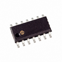
PIC16F616-I/SL Microchip Technology, PIC16F616-I/SL Datasheet - Page 91

PIC16F616-I/SL
Manufacturer Part Number
PIC16F616-I/SL
Description
IC PIC MCU FLASH 2KX14 14SOIC
Manufacturer
Microchip Technology
Series
PIC® 16Fr
Datasheets
1.PIC12F609T-ISN.pdf
(26 pages)
2.PIC16F616T-ISL.pdf
(4 pages)
3.PIC16F616T-ISL.pdf
(214 pages)
4.PIC16F616T-ISL.pdf
(8 pages)
5.PIC16F616-ESL.pdf
(180 pages)
Specifications of PIC16F616-I/SL
Program Memory Type
FLASH
Program Memory Size
3.5KB (2K x 14)
Package / Case
14-SOIC (3.9mm Width), 14-SOL
Core Processor
PIC
Core Size
8-Bit
Speed
20MHz
Peripherals
Brown-out Detect/Reset, POR, PWM, WDT
Number Of I /o
11
Ram Size
128 x 8
Voltage - Supply (vcc/vdd)
2 V ~ 5.5 V
Data Converters
A/D 8x10b
Oscillator Type
Internal
Operating Temperature
-40°C ~ 85°C
Processor Series
PIC16F
Core
PIC
Data Bus Width
8 bit
Data Ram Size
128 B
Maximum Clock Frequency
20 MHz
Number Of Programmable I/os
11
Number Of Timers
3
Maximum Operating Temperature
+ 85 C
Mounting Style
SMD/SMT
3rd Party Development Tools
52715-96, 52716-328, 52717-734
Development Tools By Supplier
PG164130, DV164035, DV244005, DV164005, PG164120, ICE2000
Minimum Operating Temperature
- 40 C
On-chip Adc
10 bit, 8 Channel
Lead Free Status / RoHS Status
Lead free / RoHS Compliant
For Use With
MCP1631RD-DCPC1 - REF DES BATT CHARG OR LED DRIVERAC162083 - HEADER MPLAB ICD2 PIC16F616 8/14
Eeprom Size
-
Connectivity
-
Lead Free Status / Rohs Status
Lead free / RoHS Compliant
Available stocks
Company
Part Number
Manufacturer
Quantity
Price
Company:
Part Number:
PIC16F616-I/SL
Manufacturer:
MICROCHIP
Quantity:
400
Company:
Part Number:
PIC16F616-I/SL
Manufacturer:
Microchip Technology
Quantity:
45 197
Part Number:
PIC16F616-I/SL
Manufacturer:
MICROCHIP
Quantity:
20 000
10.3.1
The PWM period is specified by writing to the PR2
register of Timer2. The PWM period can be calculated
using the formula of Equation 10-1.
EQUATION 10-1:
When TMR2 is equal to PR2, the following three events
occur on the next increment cycle:
• TMR2 is cleared
• The CCP1 pin is set. (Exception: If the PWM duty
• The PWM duty cycle is latched from CCPR1L into
10.3.2
The PWM duty cycle is specified by writing a 10-bit
value to multiple registers: CCPR1L register and
CCP1<1:0> bits of the CCP1CON register. The
CCPR1L contains the eight MSbs and the CCP1<1:0>
bits of the CCP1CON register contain the two LSbs.
CCPR1L and CCP1<1:0> bits of the CCP1CON
register can be written to at any time. The duty cycle
value is not latched into CCPR1H until after the period
completes (i.e., a match between PR2 and TMR2
registers occurs). While using the PWM, the CCPR1H
register is read-only.
Equation 10-2 is used to calculate the PWM pulse
width.
Equation 10-3 is used to calculate the PWM duty cycle
ratio.
TABLE 10-4:
TABLE 10-5:
© 2007 Microchip Technology Inc.
Timer Prescale (1, 4, 16)
PR2 Value
Maximum Resolution (bits)
Timer Prescale (1, 4, 16)
PR2 Value
Maximum Resolution (bits)
cycle = 0%, the pin will not be set.)
CCPR1H.
Note:
PWM Period
PWM Frequency
PWM Frequency
PWM PERIOD
The Timer2 postscaler (see Section 7.1
“Timer2 Operation”) is not used in the
determination of the PWM frequency.
PWM DUTY CYCLE
EXAMPLE PWM FREQUENCIES AND RESOLUTIONS (F
EXAMPLE PWM FREQUENCIES AND RESOLUTIONS (F
=
(TMR2 Prescale Value)
[
PWM PERIOD
(
PR2
)
+
1
] 4 T
1.22 kHz
1.22 kHz
•
0xFF
0x65
16
10
16
•
8
OSC
PIC16F610/616/16HV610/616
•
4.88 kHz
4.90 kHz
0xFF
0x65
Preliminary
10
4
4
8
19.53 kHz
19.61 kHz
EQUATION 10-2:
EQUATION 10-3:
The CCPR1H register and a 2-bit internal latch are
used to double buffer the PWM duty cycle. This double
buffering is essential for glitchless PWM operation.
The 8-bit timer TMR2 register is concatenated with
either the 2-bit internal system clock (F
the prescaler, to create the 10-bit time base. The system
clock is used if the Timer2 prescaler is set to 1:1.
When the 10-bit time base matches the CCPR1H and
2-bit latch, then the CCP1 pin is cleared (see
Figure 10-3).
10.3.3
The resolution determines the number of available duty
cycles for a given period. For example, a 10-bit resolution
will result in 1024 discrete duty cycles, whereas an 8-bit
resolution will result in 256 discrete duty cycles.
The maximum PWM resolution is 10 bits when PR2 is
255. The resolution is a function of the PR2 register
value as shown by Equation 10-4.
EQUATION 10-4:
Note:
0xFF
0x65
Duty Cycle Ratio
10
1
1
8
Pulse Width
Resolution
If the pulse width value is greater than the
period the assigned PWM pin(s) will
remain unchanged.
PWM RESOLUTION
78.12 kHz
76.92 kHz
=
0x3F
0x19
1
8
1
6
(
T
=
CCPR1L:CCP1CON<5:4>
OSC
OSC
=
OSC
PULSE WIDTH
DUTY CYCLE RATIO
PWM RESOLUTION
(
---------------------------------------------------------------------- -
CCPR1L:CCP1CON<5:4>
log
----------------------------------------- - bits
= 20 MHz)
= 8 MHz)
•
[
4 PR2
153.85 kHz
log
156.3 kHz
(
(TMR2 Prescale Value)
4 PR2
0x0C
0x1F
2 ( )
(
1
7
1
5
+
DS41288C-page 89
1
+
)
OSC
]
1
)
), or 2 bits of
208.3 kHz
200.0 kHz
0x17
0x09
)
6.6
1
1
5
•
)


