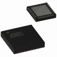
ATTINY261-20MU Atmel, ATTINY261-20MU Datasheet - Page 129

ATTINY261-20MU
Manufacturer Part Number
ATTINY261-20MU
Description
IC MCU AVR 2K FLASH 20MHZ 32-QFN
Manufacturer
Atmel
Series
AVR® ATtinyr
Specifications of ATTINY261-20MU
Core Processor
AVR
Core Size
8-Bit
Speed
20MHz
Connectivity
USI
Peripherals
Brown-out Detect/Reset, POR, PWM, WDT
Number Of I /o
16
Program Memory Size
2KB (1K x 16)
Program Memory Type
FLASH
Eeprom Size
128 x 8
Ram Size
128 x 8
Voltage - Supply (vcc/vdd)
2.7 V ~ 5.5 V
Data Converters
A/D 11x10b
Oscillator Type
Internal
Operating Temperature
-40°C ~ 85°C
Package / Case
32-VQFN Exposed Pad, 32-HVQFN, 32-SQFN, 32-DHVQFN
Processor Series
ATTINY2x
Core
AVR8
Data Bus Width
8 bit
Data Ram Size
128 B
Interface Type
2-Wire, SPI, USI
Maximum Clock Frequency
20 MHz
Number Of Programmable I/os
16
Number Of Timers
2
Maximum Operating Temperature
+ 85 C
Mounting Style
SMD/SMT
3rd Party Development Tools
EWAVR, EWAVR-BL
Development Tools By Supplier
ATAVRDRAGON, ATSTK500, ATSTK600, ATAVRISP2, ATAVRONEKIT
Minimum Operating Temperature
- 40 C
On-chip Adc
10 bit, 11 Channel
Package
32MLF EP
Device Core
AVR
Family Name
ATtiny
Maximum Speed
20 MHz
Operating Supply Voltage
3.3|5 V
For Use With
ATSTK600 - DEV KIT FOR AVR/AVR32ATAVRBC100 - REF DESIGN KIT BATTERY CHARGER770-1007 - ISP 4PORT ATMEL AVR MCU SPI/JTAGATSTK505 - ADAPTER KIT FOR 14PIN AVR MCU
Lead Free Status / RoHS Status
Lead free / RoHS Compliant
Available stocks
Company
Part Number
Manufacturer
Quantity
Price
Part Number:
ATTINY261-20MU
Manufacturer:
AVNET
Quantity:
20 000
- Current page: 129 of 242
- Download datasheet (5Mb)
13.3.3
13.3.4
2588E–AVR–08/10
SPI Slave Operation Example
Two-wire Mode
The following code demonstrates how to use the USI module as a SPI Slave:
The code is size optimized using only eight instructions (+ ret). The code example assumes that
the DO is configured as output and USCK pin is configured as input in the DDR Register. The
value stored in register r16 prior to the function is called is transferred to the master device, and
when the transfer is completed the data received from the Master is stored back into the r16
Register.
Note that the first two instructions are for initialization, only, and need only be executed once.
These instructions set three-wire mode and positive edge clock. The loop is repeated until the
USI Counter Overflow Flag is set.
The USI Two-wire mode is compliant to the Inter IC (TWI) bus protocol, but without slew rate lim-
iting on outputs and input noise filtering. Pin names used by this mode are SCL and SDA.
Figure 13-4 on page 130
one as slave. It is only the physical layer that is shown since the system operation is highly
dependent of the communication scheme used. The main differences between the master and
slave operation at this level is the serial clock generation which is always done by the master.
Only the slave uses the clock control unit.
Clock generation must be implemented in software, but the shift operation is done automatically
in both devices. Note that clocking only on negative edges for shifting data is of practical use in
this mode. The slave can insert wait states at start or end of transfer by forcing the SCL clock
low. This means that the master must always check if the SCL line was actually released after it
has generated a positive edge.
Since the clock also increments the counter, a counter overflow can be used to indicate that the
transfer is completed. The clock is generated by the master by toggling the USCK pin via the
PORTA register.
init:
...
SlaveSPITransfer:
SlaveSPITransfer_loop:
ldi
sts
sts
ldi
sts
lds
sbrs
rjmp
lds
ret
r16,(1<<USIWM0)|(1<<USICS1)
USICR,r16
USIDR,r16
r16,(1<<USIOIF)
USISR,r16
r16, USISR
r16, USIOIF
SlaveSPITransfer_loop
r16,USIDR
shows two USI units operating in two-wire mode, one as master and
129
Related parts for ATTINY261-20MU
Image
Part Number
Description
Manufacturer
Datasheet
Request
R

Part Number:
Description:
Manufacturer:
Atmel Corporation
Datasheet:

Part Number:
Description:
Manufacturer:
Atmel Corporation
Datasheet:

Part Number:
Description:
IC MCU AVR 2K FLASH 20MHZ 20-DIP
Manufacturer:
Atmel
Datasheet:

Part Number:
Description:
MCU AVR 2K FLASH 15MHZ 32-QFN
Manufacturer:
Atmel
Datasheet:

Part Number:
Description:
MCU AVR 2KB FLASH 15MHZ 32-VQFN
Manufacturer:
Atmel
Datasheet:

Part Number:
Description:
IC MCU AVR 2K FLASH 20MHZ 20SOIC
Manufacturer:
Atmel
Datasheet:

Part Number:
Description:
Attiny261 8-bit Microcontroller With 2/4/8k Bytes In-system Programmable Flash
Manufacturer:
ATMEL Corporation
Datasheet:

Part Number:
Description:
IC MCU AVR 2K FLASH 20MHZ 20SOIC
Manufacturer:
Atmel
Datasheet:

Part Number:
Description:
IC MCU AVR 2K FLASH 20MHZ 32QFN
Manufacturer:
Atmel
Datasheet:

Part Number:
Description:
Manufacturer:
Atmel Corporation
Datasheet:


