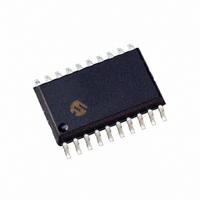
DSPIC33FJ12MC201-I/SO Microchip Technology, DSPIC33FJ12MC201-I/SO Datasheet - Page 147

DSPIC33FJ12MC201-I/SO
Manufacturer Part Number
DSPIC33FJ12MC201-I/SO
Description
IC DSPIC MCU/DSP 12K 20SOIC
Manufacturer
Microchip Technology
Series
dsPIC™ 33Fr
Datasheets
1.PIC24HJ12GP201-ISO.pdf
(84 pages)
2.DSPIC33FJ12MC201-ISO.pdf
(288 pages)
3.DSPIC33FJ12MC201-ISO.pdf
(14 pages)
4.DSPIC33FJ12MC201-IP.pdf
(284 pages)
Specifications of DSPIC33FJ12MC201-I/SO
Program Memory Type
FLASH
Program Memory Size
12KB (12K x 8)
Package / Case
20-SOIC (7.5mm Width)
Core Processor
dsPIC
Core Size
16-Bit
Speed
40 MIPs
Connectivity
I²C, IrDA, SPI, UART/USART
Peripherals
Brown-out Detect/Reset, Motor Control PWM, QEI, POR, PWM, WDT
Number Of I /o
15
Ram Size
1K x 8
Voltage - Supply (vcc/vdd)
3 V ~ 3.6 V
Data Converters
A/D 4x10b
Oscillator Type
Internal
Operating Temperature
-40°C ~ 85°C
Product
DSCs
Data Bus Width
16 bit
Processor Series
DSPIC33F
Core
dsPIC
Maximum Clock Frequency
40 MHz
Number Of Programmable I/os
15
Data Ram Size
1 KB
Maximum Operating Temperature
+ 85 C
Mounting Style
SMD/SMT
3rd Party Development Tools
52713-733, 52714-737, 53276-922, EWDSPIC
Development Tools By Supplier
PG164130, DV164035, DV244005, DV164005, PG164120, DM240001, DV164033
Minimum Operating Temperature
- 40 C
Lead Free Status / RoHS Status
Lead free / RoHS Compliant
For Use With
DV164033 - KIT START EXPLORER 16 MPLAB ICD2DM240001 - BOARD DEMO PIC24/DSPIC33/PIC32
Eeprom Size
-
Lead Free Status / Rohs Status
Lead free / RoHS Compliant
- PIC24HJ12GP201-ISO PDF datasheet
- DSPIC33FJ12MC201-ISO PDF datasheet #2
- DSPIC33FJ12MC201-ISO PDF datasheet #3
- DSPIC33FJ12MC201-IP PDF datasheet #4
- Current page: 147 of 288
- Download datasheet (5Mb)
13.0
The Input Capture module is useful in applications
requiring frequency (period) and pulse measurement.
The dsPIC33FJ12MC201/202 devices support up to
eight input capture channels.
The Input Capture module captures the 16-bit value of
the selected Time Base register when an event occurs
at the ICx pin. The events that cause a capture event
are listed below in three categories:
1.
2.
FIGURE 13-1:
© 2009 Microchip Technology Inc.
Note:
- Capture timer value on every falling edge of
- Capture timer value on every rising edge of
Note: An ‘x’ in a signal, register or bit name denotes the number of the capture channel.
ICx Pin
Simple Capture Event modes:
input at ICx pin
input at ICx pin
Capture timer value on every edge (rising and
falling)
INPUT CAPTURE
This data sheet summarizes the features
of the dsPIC33FJ12MC201/202 family of
devices. It is not intended to be a
comprehensive
complement the information in this data
sheet, refer to the “dsPIC33F Family Ref-
erence Manual”, Section 12. “Input Cap-
ture” (DS70198), which is available from
the
(www.microchip.com).
Prescaler
(1, 4, 16)
Counter
3
Microchip
INPUT CAPTURE BLOCK DIAGRAM
System Bus
ICxCON
ICM<2:0> (ICxCON<2:0>)
reference
ICOV, ICBNE (ICxCON<4:3>)
Mode Select
Edge Detection Logic
web
Clock Synchronizer
source.
ICxI<1:0>
and
site
Preliminary
To
dsPIC33FJ12MC201/202
(in IFSn Register)
Set Flag ICxIF
Interrupt
Logic
3.
Each Input Capture channel can select one of two
16-bit timers (Timer2 or Timer3) for the time base.
The selected timer can use either an internal or
external clock.
Other operational features include:
• Device wake-up from capture pin during CPU
• Interrupt on Input Capture event
• 4-word FIFO buffer for capture values
• Use of Input Capture to provide additional
- Capture timer value on every 4th rising edge
- Capture timer value on every 16th rising
Sleep and Idle modes
- Interrupt optionally generated after 1, 2, 3, or
sources of external interrupts
Prescaler Capture Event modes:
of input at ICx pin
edge of input at ICx pin
4 buffer locations are filled
Logic
FIFO
R/W
From 16-bit Timers
TMR2 TMR3
1
ICxBUF
16
0
DS70265D-page 145
16
ICTMR
(ICxCON<7>)
Related parts for DSPIC33FJ12MC201-I/SO
Image
Part Number
Description
Manufacturer
Datasheet
Request
R

Part Number:
Description:
IC, DSC, 16BIT, 12KB, 40MHZ, 3.6V, DIP28
Manufacturer:
Microchip Technology
Datasheet:

Part Number:
Description:
Manufacturer:
Microchip Technology Inc.
Datasheet:

Part Number:
Description:
Manufacturer:
Microchip Technology Inc.
Datasheet:

Part Number:
Description:
Manufacturer:
Microchip Technology Inc.
Datasheet:

Part Number:
Description:
Manufacturer:
Microchip Technology Inc.
Datasheet:

Part Number:
Description:
Manufacturer:
Microchip Technology Inc.
Datasheet:

Part Number:
Description:
Manufacturer:
Microchip Technology Inc.
Datasheet:

Part Number:
Description:
Manufacturer:
Microchip Technology Inc.
Datasheet:

Part Number:
Description:
Manufacturer:
Microchip Technology Inc.
Datasheet:


