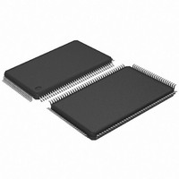
AT91SAM7L64-AU Atmel, AT91SAM7L64-AU Datasheet - Page 162

AT91SAM7L64-AU
Manufacturer Part Number
AT91SAM7L64-AU
Description
MCU ARM7 64K HS FLASH 128-LQFP
Manufacturer
Atmel
Series
AT91SAMr
Specifications of AT91SAM7L64-AU
Core Processor
ARM7
Core Size
16/32-Bit
Speed
36MHz
Connectivity
I²C, SPI, UART/USART
Peripherals
Brown-out Detect/Reset, LCD, POR, PWM, WDT
Number Of I /o
80
Program Memory Size
64KB (64K x 8)
Program Memory Type
FLASH
Ram Size
6K x 8
Voltage - Supply (vcc/vdd)
1.55 V ~ 1.8 V
Data Converters
A/D 4x10b
Oscillator Type
Internal
Operating Temperature
-40°C ~ 85°C
Package / Case
128-LQFP
Controller Family/series
AT91SAM7xxx
No. Of I/o's
80
Ram Memory Size
6KB
Cpu Speed
36MHz
No. Of Timers
1
Rohs Compliant
Yes
Processor Series
AT91SAMx
Core
ARM7TDMI
Data Bus Width
32 bit
Data Ram Size
6 KB
Interface Type
2-Wire, SPI, USART
Maximum Clock Frequency
36 MHz
Number Of Programmable I/os
80
Number Of Timers
3
Maximum Operating Temperature
+ 85 C
Mounting Style
SMD/SMT
3rd Party Development Tools
JTRACE-ARM-2M, MDK-ARM, RL-ARM, ULINK2
Development Tools By Supplier
AT91SAM-ICE, AT91-ISP, AT91SAM7L-EK
Minimum Operating Temperature
- 40 C
On-chip Adc
10 bit, 4 Channel
For Use With
AT91SAM7L-STK - KIT EVAL FOR AT91SAM7LAT91SAM-ICE - EMULATOR FOR AT91 ARM7/ARM9
Lead Free Status / RoHS Status
Lead free / RoHS Compliant
Eeprom Size
-
Lead Free Status / Rohs Status
Details
Available stocks
Company
Part Number
Manufacturer
Quantity
Price
- Current page: 162 of 564
- Download datasheet (9Mb)
Table 20-5.
20.2.5
20.2.5.1
20.2.5.2
162
Step
9
10
11
12
13
AT91SAM7L128/64 Preliminary
Device Operations
Programmer Action
Sets NOE signal
Waits for NVALID high
Sets DATA in output mode
Sets NCMD signal
Waits for RDY high
Flash Read Command
Flash Write Command
Read Handshake (Continued)
Several commands on the Flash memory are available. These commands are summarized in
Table 20-3 on page
face running several read/write handshaking sequences.
When a new command is executed, the previous one is automatically achieved. Thus, chaining
a read command after a write automatically flushes the load buffer in the Flash.
This command is used to read the contents of the Flash memory. The read command can start
at any valid address in the memory plane and is optimized for consecutive reads. Read hand-
shaking can be chained; an internal address buffer is automatically increased.
Table 20-6.
This command is used to write the Flash contents.
The Flash memory plane is organized into several pages. Data to be written are stored in a load
buffer that corresponds to a Flash memory page. The load buffer is automatically flushed to the
Flash:
Step
1
2
3
4
5
...
n
n+1
n+2
n+3
...
• before access to any page other than the current one
• when a new command is validated (MODE = CMDE)
Handshake Sequence
Write handshaking
Write handshaking
Write handshaking
Read handshaking
Read handshaking
...
Write handshaking
Write handshaking
Read handshaking
Read handshaking
...
Read Command
159. Each command is driven by the programmer through the parallel inter-
Sets NVALID signal
Waits for NCMD high
Sets RDY signal
Device Action
Sets DATA bus in input mode
MODE[3:0]
CMDE
ADDR0
ADDR1
DATA
DATA
...
ADDR0
ADDR1
DATA
DATA
...
DATA[15:0]
READ
Memory Address LSB
Memory Address
*Memory Address++
*Memory Address++
...
Memory Address
*Memory Address++
*Memory Address++
...
Memory Address LSB
DATA I/O
Output
X
Input
Input
Input
6257A–ATARM–20-Feb-08
Related parts for AT91SAM7L64-AU
Image
Part Number
Description
Manufacturer
Datasheet
Request
R

Part Number:
Description:
KIT EVAL FOR AT91SAM7L
Manufacturer:
Atmel
Datasheet:

Part Number:
Description:
DEV KIT FOR AVR/AVR32
Manufacturer:
Atmel
Datasheet:

Part Number:
Description:
INTERVAL AND WIPE/WASH WIPER CONTROL IC WITH DELAY
Manufacturer:
ATMEL Corporation
Datasheet:

Part Number:
Description:
Low-Voltage Voice-Switched IC for Hands-Free Operation
Manufacturer:
ATMEL Corporation
Datasheet:

Part Number:
Description:
MONOLITHIC INTEGRATED FEATUREPHONE CIRCUIT
Manufacturer:
ATMEL Corporation
Datasheet:

Part Number:
Description:
AM-FM Receiver IC U4255BM-M
Manufacturer:
ATMEL Corporation
Datasheet:

Part Number:
Description:
Monolithic Integrated Feature Phone Circuit
Manufacturer:
ATMEL Corporation
Datasheet:

Part Number:
Description:
Multistandard Video-IF and Quasi Parallel Sound Processing
Manufacturer:
ATMEL Corporation
Datasheet:

Part Number:
Description:
High-performance EE PLD
Manufacturer:
ATMEL Corporation
Datasheet:

Part Number:
Description:
8-bit Flash Microcontroller
Manufacturer:
ATMEL Corporation
Datasheet:

Part Number:
Description:
2-Wire Serial EEPROM
Manufacturer:
ATMEL Corporation
Datasheet:


