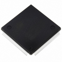
ST10F269Z2Q3 STMicroelectronics, ST10F269Z2Q3 Datasheet - Page 17

ST10F269Z2Q3
Manufacturer Part Number
ST10F269Z2Q3
Description
IC FLASH MEM 256KBIT 144-PQFP
Manufacturer
STMicroelectronics
Series
ST10r
Datasheet
1.ST10F269Z2Q3.pdf
(184 pages)
Specifications of ST10F269Z2Q3
Core Processor
ST10
Core Size
16-Bit
Speed
40MHz
Connectivity
CAN, EBI/EMI, SSC, UART/USART
Peripherals
POR, PWM, WDT
Number Of I /o
111
Program Memory Size
256KB (256K x 8)
Program Memory Type
FLASH
Ram Size
12K x 8
Voltage - Supply (vcc/vdd)
4.5 V ~ 5.5 V
Data Converters
A/D 16x10b
Oscillator Type
Internal
Operating Temperature
-40°C ~ 125°C
Package / Case
144-QFP
Processor Series
ST10F26x
Core
ST10
Data Bus Width
16 bit
Data Ram Size
12 KB
Interface Type
CAN, SSC, USART
Maximum Clock Frequency
40 MHz
Number Of Programmable I/os
111
Number Of Timers
2 x 16 bit
Operating Supply Voltage
0.3 V to 4 V
Maximum Operating Temperature
+ 125 C
Mounting Style
SMD/SMT
Minimum Operating Temperature
- 40 C
On-chip Adc
16 bit x 10 bit
Cpu Family
ST10
Device Core Size
16b
Frequency (max)
40MHz
Total Internal Ram Size
12KB
# I/os (max)
111
Number Of Timers - General Purpose
5
Operating Supply Voltage (typ)
5V
Operating Supply Voltage (max)
5.5V
Operating Supply Voltage (min)
4.5V
Instruction Set Architecture
CISC/RISC
Operating Temp Range
-40C to 125C
Operating Temperature Classification
Automotive
Mounting
Surface Mount
Pin Count
144
Package Type
PQFP
Lead Free Status / RoHS Status
Lead free / RoHS Compliant
Eeprom Size
-
Lead Free Status / Rohs Status
Lead free / RoHS Compliant
Other names
497-2042
Available stocks
Company
Part Number
Manufacturer
Quantity
Price
Company:
Part Number:
ST10F269Z2Q3
Manufacturer:
INFINEON
Quantity:
1 443
Company:
Part Number:
ST10F269Z2Q3
Manufacturer:
STMicroelectronics
Quantity:
10 000
Part Number:
ST10F269Z2Q3
Manufacturer:
ST
Quantity:
20 000
ST10F269
5 - INTERNAL FLASH MEMORY
5.1 - Overview
– 128K or 256K Byte on-chip Flash memory
– Two possibilities of Flash mapping into the CPU
– Flash memory can be used for code and data
– 32-bit, zero waitstate read access (50ns cycle
– Erase-Program Controller (EPC) similar to
– Memory Erase in blocks
Table 2 : 128K or 256K Byte Flash Memory Block Organization
*Not available on 128K versions (reserved areas).
• Word-by-Word Programmable (16 s typical)
• Data polling and Toggle Protocol for EPC
• Ready/Busy signal connected on XP2INT
• Internal Power-On detection circuit
• One 16K Byte, two 8K Byte, one 32K Byte, one
• Each
• Chip erase (8.5 second typical)
• Each block can be separately protected
• Each protected block can be temporary unpro-
• When enabled, the read protection prevents
address space
storage
time at f
62.5ns cycle time at f
devices)
M29F400B STM’s stand-alone Flash memory
Status
interrupt line
to three 64K Byte blocks
(1.5 second typical)
against programming and erasing
tected
access to data in Flash memory using a pro-
gram running out of the Flash memory space.
CPU
Block
block
5*
6*
0
1
2
3
4
= 40MHz on PQFP144 devices and
can
CPU
be
= 32MHz on TQFP144
Addresses (Segment 0)
03’0000h to 03’FFFFh*
04’0000h to 04’FFFFh*
00’0000h to 00’3FFFh
00’4000h to 00’5FFFh
00’6000h to 00’7FFFh
01’8000h to 01’FFFFh
02’0000h to 02’FFFFh
erased
separately
Addresses (Segment 1)
– Erase Suspend and Resume Modes
– Single Voltage operation, no need of dedicated
– Low Power Consumption:
– 1000 Erase-Program Cycles per block, 20 years
– Operating temperature: -40 to +125
5.2 - Operational Overview
Read Mode
In standard mode (the normal operating mode)
the Flash appears like an on-chip ROM with the
same timing and functionality. The Flash module
offers a fast access time, allowing zero waitstate
access with CPU frequency up to 40MHz on
PQFP144 devices and up to 32MHz on TQFP144
devices. Instruction fetches and data operand
reads are performed with all addressing modes of
the ST10F269 instruction set.
In order to optimize the programming time of the
internal Flash, blocks of 8K Bytes, 16K Bytes,
32K Bytes, 64K Bytes can be used. But the size of
the blocks does not apply to the whole memory
space, see details in Table 2.
03’0000h to 03’FFFFh*
04’0000h to 04’FFFFh*
01’0000h to 01’3FFFh
01’4000h to 01’5FFFh
01’6000h to 01’7FFFh
01’8000h to 01’FFFFh
02’0000h to 02’FFFFh
• Read and Program another Block during erase
• 45mA max. Read current
• 60mA max. Program or Erase current
• Automatic Stand-by-mode (50 A maximum)
Access to data of internal Flash can only be per-
formed with an inner protected program
suspend
supply pin
of data retention time
+125
o
C
5 - INTERNAL FLASH MEMORY
Size (byte)
64K*
64K*
16K
32K
64K
8K
8K
o
C / -40 to
17/184


