C8051F305-GM Silicon Laboratories Inc, C8051F305-GM Datasheet - Page 35
C8051F305-GM
Manufacturer Part Number
C8051F305-GM
Description
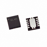
IC 8051 MCU 2K FLASH 11QFN
Manufacturer
Silicon Laboratories Inc
Series
C8051F30xr
Specifications of C8051F305-GM
Program Memory Type
FLASH
Program Memory Size
2KB (2K x 8)
Package / Case
11-VQFN
Core Processor
8051
Core Size
8-Bit
Speed
25MHz
Connectivity
SMBus (2-Wire/I²C), UART/USART
Peripherals
POR, PWM, WDT
Number Of I /o
8
Ram Size
256 x 8
Voltage - Supply (vcc/vdd)
2.7 V ~ 3.6 V
Oscillator Type
External
Operating Temperature
-40°C ~ 85°C
Processor Series
C8051F3x
Core
8051
Data Bus Width
8 bit
Data Ram Size
256 B
Interface Type
I2C/SMBus/UART
Maximum Clock Frequency
25 MHz
Number Of Programmable I/os
8
Number Of Timers
3
Operating Supply Voltage
2.7 V to 3.6 V
Maximum Operating Temperature
+ 85 C
Mounting Style
SMD/SMT
3rd Party Development Tools
PK51, CA51, A51, ULINK2
Development Tools By Supplier
C8051F300DK
Minimum Operating Temperature
- 40 C
On-chip Adc
8 bit, 8 Channel
No. Of I/o's
8
Ram Memory Size
256Byte
Cpu Speed
25MHz
No. Of Timers
3
Rohs Compliant
Yes
Package
11QFN EP
Device Core
8051
Family Name
C8051F30x
Maximum Speed
25 MHz
Lead Free Status / RoHS Status
Lead free / RoHS Compliant
For Use With
770-1006 - ISP 4PORT FOR SILABS C8051F MCU336-1444 - ADAPTER PROGRAM TOOLSTICK F300
Eeprom Size
-
Data Converters
-
Lead Free Status / Rohs Status
Lead free / RoHS Compliant
Other names
336-1251
Available stocks
Company
Part Number
Manufacturer
Quantity
Price
Company:

Part Number:
C8051F305-GM
Manufacturer:
SiliconL
Quantity:
162
Part Number:
C8051F305-GMR
Manufacturer:
SILICONLABS/芯科
Quantity:
20 000


5.
The ADC0 subsystem for the C8051F300/2 consists of two analog multiplexers (referred to collectively as
AMUX0) with 11 total input selections, a differential programmable gain amplifier (PGA), and a 500 ksps, 8-
bit successive-approximation-register ADC with integrated track-and-hold and programmable window
detector (see block diagram in Figure 5.1). The AMUX0, PGA, data conversion modes, and window detec-
tor are all configurable under software control via the Special Function Registers shown in Figure 5.1.
ADC0 operates in both Single-ended and Differential modes, and may be configured to measure any Port
pin, the Temperature Sensor output, or V
enabled only when the AD0EN bit in the ADC0 Control register (ADC0CN) is set to logic 1. The ADC0 sub-
system is in low power shutdown when this bit is logic 0.
Sensor
Temp
ADC0 (8-Bit ADC, C8051F300/2)
GND
P0.0
P0.1
P0.2
P0.3
P0.4
P0.5
P0.6
P0.7
VDD
P0.0
P0.1
P0.2
P0.3
P0.4
P0.5
P0.6
P0.7
AMUX0
Figure 5.1. ADC0 Functional Block Diagram
10-to-1
AMUX
AMUX
9-to-1
DD
with respect to any Port pin or GND. The ADC0 subsystem is
X
Rev. 2.9
+
-
AMX0SL
VDD
ADC0CF
C8051F300/1/2/3/4/5
ADC
VDD
8-Bit
SAR
ADC0GT
ADC0LT
ADC0CN
Conversion
Start
16
8
000
001
010
011
1xx
AD0WINT
Comb.
AD0BUSY (W)
Timer 0 Overflow
Timer 2 Overflow
Timer 1 Overflow
CNVSTR Input
Logic
35
Related parts for C8051F305-GM
Image
Part Number
Description
Manufacturer
Datasheet
Request
R

Part Number:
Description:
SMD/C°/SINGLE-ENDED OUTPUT SILICON OSCILLATOR
Manufacturer:
Silicon Laboratories Inc
Part Number:
Description:
Manufacturer:
Silicon Laboratories Inc
Datasheet:
Part Number:
Description:
N/A N/A/SI4010 AES KEYFOB DEMO WITH LCD RX
Manufacturer:
Silicon Laboratories Inc
Datasheet:
Part Number:
Description:
N/A N/A/SI4010 SIMPLIFIED KEY FOB DEMO WITH LED RX
Manufacturer:
Silicon Laboratories Inc
Datasheet:
Part Number:
Description:
N/A/-40 TO 85 OC/EZLINK MODULE; F930/4432 HIGH BAND (REV E/B1)
Manufacturer:
Silicon Laboratories Inc
Part Number:
Description:
EZLink Module; F930/4432 Low Band (rev e/B1)
Manufacturer:
Silicon Laboratories Inc
Part Number:
Description:
I°/4460 10 DBM RADIO TEST CARD 434 MHZ
Manufacturer:
Silicon Laboratories Inc
Part Number:
Description:
I°/4461 14 DBM RADIO TEST CARD 868 MHZ
Manufacturer:
Silicon Laboratories Inc
Part Number:
Description:
I°/4463 20 DBM RFSWITCH RADIO TEST CARD 460 MHZ
Manufacturer:
Silicon Laboratories Inc
Part Number:
Description:
I°/4463 20 DBM RADIO TEST CARD 868 MHZ
Manufacturer:
Silicon Laboratories Inc
Part Number:
Description:
I°/4463 27 DBM RADIO TEST CARD 868 MHZ
Manufacturer:
Silicon Laboratories Inc
Part Number:
Description:
I°/4463 SKYWORKS 30 DBM RADIO TEST CARD 915 MHZ
Manufacturer:
Silicon Laboratories Inc
Part Number:
Description:
N/A N/A/-40 TO 85 OC/4463 RFMD 30 DBM RADIO TEST CARD 915 MHZ
Manufacturer:
Silicon Laboratories Inc
Part Number:
Description:
I°/4463 20 DBM RADIO TEST CARD 169 MHZ
Manufacturer:
Silicon Laboratories Inc