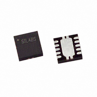
C8051F305-GM Silicon Laboratories Inc, C8051F305-GM Datasheet - Page 39

C8051F305-GM
Manufacturer Part Number
C8051F305-GM
Description
IC 8051 MCU 2K FLASH 11QFN
Manufacturer
Silicon Laboratories Inc
Series
C8051F30xr
Specifications of C8051F305-GM
Program Memory Type
FLASH
Program Memory Size
2KB (2K x 8)
Package / Case
11-VQFN
Core Processor
8051
Core Size
8-Bit
Speed
25MHz
Connectivity
SMBus (2-Wire/I²C), UART/USART
Peripherals
POR, PWM, WDT
Number Of I /o
8
Ram Size
256 x 8
Voltage - Supply (vcc/vdd)
2.7 V ~ 3.6 V
Oscillator Type
External
Operating Temperature
-40°C ~ 85°C
Processor Series
C8051F3x
Core
8051
Data Bus Width
8 bit
Data Ram Size
256 B
Interface Type
I2C/SMBus/UART
Maximum Clock Frequency
25 MHz
Number Of Programmable I/os
8
Number Of Timers
3
Operating Supply Voltage
2.7 V to 3.6 V
Maximum Operating Temperature
+ 85 C
Mounting Style
SMD/SMT
3rd Party Development Tools
PK51, CA51, A51, ULINK2
Development Tools By Supplier
C8051F300DK
Minimum Operating Temperature
- 40 C
On-chip Adc
8 bit, 8 Channel
No. Of I/o's
8
Ram Memory Size
256Byte
Cpu Speed
25MHz
No. Of Timers
3
Rohs Compliant
Yes
Package
11QFN EP
Device Core
8051
Family Name
C8051F30x
Maximum Speed
25 MHz
Lead Free Status / RoHS Status
Lead free / RoHS Compliant
For Use With
770-1006 - ISP 4PORT FOR SILABS C8051F MCU336-1444 - ADAPTER PROGRAM TOOLSTICK F300
Eeprom Size
-
Data Converters
-
Lead Free Status / Rohs Status
Lead free / RoHS Compliant
Other names
336-1251
Available stocks
Company
Part Number
Manufacturer
Quantity
Price
Company:
Part Number:
C8051F305-GM
Manufacturer:
SiliconL
Quantity:
162
Part Number:
C8051F305-GMR
Manufacturer:
SILICONLABS/芯科
Quantity:
20 000
5.3.
ADC0 has a maximum conversion speed of 500 ksps. The ADC0 conversion clock is a divided version of
the system clock, determined by the AD0SC bits in the ADC0CF register (system clock divided by
(AD0SC + 1) for 0 AD0SC 31).
5.3.1. Starting a Conversion
A conversion can be initiated in one of five ways, depending on the programmed states of the ADC0 Start
of Conversion Mode bits (AD0CM2–0) in register ADC0CN. Conversions may be initiated by one of the fol-
lowing:
Writing a ‘1’ to AD0BUSY provides software control of ADC0 whereby conversions are performed "on-
demand". During conversion, the AD0BUSY bit is set to logic 1 and reset to logic 0 when the conversion is
complete. The falling edge of AD0BUSY triggers an interrupt (when enabled) and sets the ADC0 interrupt
flag (AD0INT). Note: When polling for ADC conversion completions, the ADC0 interrupt flag (AD0INT)
should be used. Converted data is available in the ADC0 data register, ADC0, when bit AD0INT is logic 1.
Note that when Timer 2 overflows are used as the conversion source, Timer 2 Low Byte overflows are
used if Timer 2 is in 8-bit mode; Timer 2 High byte overflows are used if Timer 2 is in 16-bit mode. See
tion “15. Timers” on page 143
Important Note About Using CNVSTR: The CNVSTR input pin also functions as Port pin P0.6. When the
CNVSTR input is used as the ADC0 conversion source, Port pin P0.6 should be skipped by the Digital
Crossbar. To configure the Crossbar to skip P0.6, set to ‘1’ Bit6 in register XBR0. See
Input/Output” on page 103
Modes of Operation
1. Writing a ‘1’ to the AD0BUSY bit of register ADC0CN
2. A Timer 0 overflow (i.e. timed continuous conversions)
3. A Timer 2 overflow
4. A Timer 1 overflow
5. A rising edge on the CNVSTR input signal (pin P0.6)
for details on Port I/O configuration.
for timer configuration.
Rev. 2.9
C8051F300/1/2/3/4/5
Section “12. Port
Sec-
39


