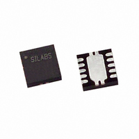
C8051F305-GM Silicon Laboratories Inc, C8051F305-GM Datasheet - Page 64

C8051F305-GM
Manufacturer Part Number
C8051F305-GM
Description
IC 8051 MCU 2K FLASH 11QFN
Manufacturer
Silicon Laboratories Inc
Series
C8051F30xr
Specifications of C8051F305-GM
Program Memory Type
FLASH
Program Memory Size
2KB (2K x 8)
Package / Case
11-VQFN
Core Processor
8051
Core Size
8-Bit
Speed
25MHz
Connectivity
SMBus (2-Wire/I²C), UART/USART
Peripherals
POR, PWM, WDT
Number Of I /o
8
Ram Size
256 x 8
Voltage - Supply (vcc/vdd)
2.7 V ~ 3.6 V
Oscillator Type
External
Operating Temperature
-40°C ~ 85°C
Processor Series
C8051F3x
Core
8051
Data Bus Width
8 bit
Data Ram Size
256 B
Interface Type
I2C/SMBus/UART
Maximum Clock Frequency
25 MHz
Number Of Programmable I/os
8
Number Of Timers
3
Operating Supply Voltage
2.7 V to 3.6 V
Maximum Operating Temperature
+ 85 C
Mounting Style
SMD/SMT
3rd Party Development Tools
PK51, CA51, A51, ULINK2
Development Tools By Supplier
C8051F300DK
Minimum Operating Temperature
- 40 C
On-chip Adc
8 bit, 8 Channel
No. Of I/o's
8
Ram Memory Size
256Byte
Cpu Speed
25MHz
No. Of Timers
3
Rohs Compliant
Yes
Package
11QFN EP
Device Core
8051
Family Name
C8051F30x
Maximum Speed
25 MHz
Lead Free Status / RoHS Status
Lead free / RoHS Compliant
For Use With
770-1006 - ISP 4PORT FOR SILABS C8051F MCU336-1444 - ADAPTER PROGRAM TOOLSTICK F300
Eeprom Size
-
Data Converters
-
Lead Free Status / Rohs Status
Lead free / RoHS Compliant
Other names
336-1251
Available stocks
Company
Part Number
Manufacturer
Quantity
Price
Company:
Part Number:
C8051F305-GM
Manufacturer:
SiliconL
Quantity:
162
Part Number:
C8051F305-GMR
Manufacturer:
SILICONLABS/芯科
Quantity:
20 000
C8051F300/1/2/3/4/5
8.2.2. Data Memory
The CIP-51 includes 256 bytes of internal RAM mapped into the data memory space from 0x00 through
0xFF. The lower 128 bytes of data memory are used for general purpose registers and scratch pad mem-
ory. Either direct or indirect addressing may be used to access the lower 128 bytes of data memory. Loca-
tions 0x00 through 0x1F are addressable as four banks of general purpose registers, each bank consisting
of eight byte-wide registers. The next 16 bytes, locations 0x20 through 0x2F, may either be addressed as
bytes or as 128 bit locations accessible with the direct addressing mode.
The upper 128 bytes of data memory are accessible only by indirect addressing. This region occupies the
same address space as the Special Function Registers (SFR) but is physically separate from the SFR
space. The addressing mode used by an instruction when accessing locations above 0x7F determines
whether the CPU accesses the upper 128 bytes of data memory space or the SFRs. Instructions that use
direct addressing will access the SFR space. Instructions using indirect addressing above 0x7F access the
upper 128 bytes of data memory. Figure 8.3 illustrates the data memory organization of the CIP-51.
8.2.3. General Purpose Registers
The lower 32 bytes of data memory, locations 0x00 through 0x1F, may be addressed as four banks of gen-
eral-purpose registers. Each bank consists of eight byte-wide registers designated R0 through R7. Only
one of these banks may be enabled at a time. Two bits in the program status word, RS0 (PSW.3) and RS1
(PSW.4), select the active register bank (see description of the PSW in SFR Definition 8.4). This allows
fast context switching when entering subroutines and interrupt service routines. Indirect addressing modes
use registers R0 and R1 as index registers.
64
0xFF
0x7F
0x2F
0x1F
0x80
0x30
0x20
0x00
(Indirect Addressing
(Direct and Indirect
Figure 8.3. Data Memory Map
General Purpose
INTERNAL DATA ADDRESS SPACE
Upper 128 RAM
Bit Addressable
Addressing)
Registers
Only)
Rev. 2.9
(Direct Addressing Only)
Special Function
Lower 128 RAM
(Direct and Indirect
Addressing)
Register's


