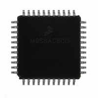
MC9S08AC8CFGE Freescale Semiconductor, MC9S08AC8CFGE Datasheet - Page 85

MC9S08AC8CFGE
Manufacturer Part Number
MC9S08AC8CFGE
Description
IC MCU 8BIT 8K FLASH 44-LQFP
Manufacturer
Freescale Semiconductor
Series
HCS08r
Datasheet
1.MC9S08AC8CFGE.pdf
(336 pages)
Specifications of MC9S08AC8CFGE
Core Processor
HCS08
Core Size
8-Bit
Speed
40MHz
Connectivity
I²C, SCI, SPI
Peripherals
LVD, POR, PWM, WDT
Number Of I /o
34
Program Memory Size
8KB (8K x 8)
Program Memory Type
FLASH
Ram Size
768 x 8
Voltage - Supply (vcc/vdd)
2.7 V ~ 5.5 V
Data Converters
A/D 8x10b
Oscillator Type
Internal
Operating Temperature
-40°C ~ 85°C
Package / Case
44-LQFP
Processor Series
S08AC
Core
HCS08
Data Bus Width
8 bit
Data Ram Size
700 B
Interface Type
I2C, SCI, SPI
Maximum Clock Frequency
40 MHz
Number Of Programmable I/os
34
Number Of Timers
3
Operating Supply Voltage
- 0.3 V to + 5.8 V
Maximum Operating Temperature
+ 125 C
Mounting Style
SMD/SMT
3rd Party Development Tools
EWS08
Development Tools By Supplier
DEMO9S08AC60E, DEMOACEX, DEMOACKIT, DCF51AC256, DC9S08AC128, DC9S08AC16, DC9S08AC60, DEMO51AC256KIT
Minimum Operating Temperature
- 40 C
On-chip Adc
10 bit, 8 Channel
Lead Free Status / RoHS Status
Lead free / RoHS Compliant
Eeprom Size
-
Lead Free Status / Rohs Status
Lead free / RoHS Compliant
Available stocks
Company
Part Number
Manufacturer
Quantity
Price
Company:
Part Number:
MC9S08AC8CFGE
Manufacturer:
Freescale Semiconductor
Quantity:
10 000
- Current page: 85 of 336
- Download datasheet (7Mb)
6.3.4
Port D pins are general-purpose I/O pins. Parallel I/O function is controlled by the port D data (PTDD) and
data direction (PTDDD) registers which are located in page zero register space. The pin control registers,
pullup enable (PTDPE), slew rate control (PTDSE), and drive strength select (PTDDS) are located in the
high page registers. Refer to
general-purpose I/O control and
Port D general-purpose I/O are shared with the ADC and KBI. When any of these shared functions is
enabled, the direction, input or output, is controlled by the shared function and not by the data direction
register of the parallel I/O port. When a pin is shared with both the ADC and a digital peripheral function,
the ADC has higher priority. For example, in the case that both the ADC and the KBI are configured to
use PTD7 then the pin is controlled by the ADC module.
Refer to
external clock inputs.
Refer to
port D pins as analog inputs.
Refer to
keyboard inputs.
6.3.5
Port E pins are general-purpose I/O pins. Parallel I/O function is controlled by the port E data (PTED) and
data direction (PTEDD) registers which are located in page zero register space. The pin control registers,
pullup enable (PTEPE), slew rate control (PTESE), and drive strength select (PTEDS) are located in the
high page registers. Refer to
general-purpose I/O control and
Port E general-purpose I/O is shared with SCI1, SPI, and TPM1 timer channels. When any of these shared
functions is enabled, the direction, input or output, is controlled by the shared function and not by the data
direction register of the parallel I/O port. Also, for pins which are configured as outputs by the shared
function, the output data is controlled by the shared function and not by the port data register.
Freescale Semiconductor
Port E
Port D
Chapter 10, “Timer/PWM
Chapter 14, “Analog-to-Digital Converter
Chapter 9, “Keyboard Interrupt
Port D
Port E
MCU Pin:
MCU Pin:
SPSCK1
PTE7/
Bit 7
Section 6.4, “Parallel I/O
Section 6.4, “Parallel I/O
Bit 7
R
Section 6.5, “Pin
Section 6.5, “Pin
MOSI1
PTE6/
MC9S08AC16 Series Data Sheet, Rev. 8
(S08TPMV3)” for more information about using port D pins as TPM
6
Figure 6-5. Port D Pin Names
Figure 6-6. Port E Pin Names
R
6
(S08KBIV1)” for more information about using port D pins as
MISO1
PTE5/
5
R
5
Control” for more information about pin control.
Control” for more information about pin control.
(S08ADC10V1)” for more information about using
Control” for more information about
PTE4/
Control” for more information about
SS1
4
R
4
TPM1CH1
AD1P11/
PTD3/
KBIP6
PTE3/
3
3
AD1P10/
TPM1CH0
PTD2/
KBIP5
PTE2/
2
2
Chapter 6 Parallel Input/Output
AD1P9
PTD1/
1
PTE1/
RxD1
1
AD1P8
PTD0/
Bit 0
PTE0/
TxD1
Bit 0
85
Related parts for MC9S08AC8CFGE
Image
Part Number
Description
Manufacturer
Datasheet
Request
R
Part Number:
Description:
Manufacturer:
Freescale Semiconductor, Inc
Datasheet:
Part Number:
Description:
Manufacturer:
Freescale Semiconductor, Inc
Datasheet:
Part Number:
Description:
Manufacturer:
Freescale Semiconductor, Inc
Datasheet:
Part Number:
Description:
Manufacturer:
Freescale Semiconductor, Inc
Datasheet:
Part Number:
Description:
Manufacturer:
Freescale Semiconductor, Inc
Datasheet:
Part Number:
Description:
Manufacturer:
Freescale Semiconductor, Inc
Datasheet:
Part Number:
Description:
Manufacturer:
Freescale Semiconductor, Inc
Datasheet:
Part Number:
Description:
Manufacturer:
Freescale Semiconductor, Inc
Datasheet:
Part Number:
Description:
Manufacturer:
Freescale Semiconductor, Inc
Datasheet:
Part Number:
Description:
Manufacturer:
Freescale Semiconductor, Inc
Datasheet:
Part Number:
Description:
Manufacturer:
Freescale Semiconductor, Inc
Datasheet:
Part Number:
Description:
Manufacturer:
Freescale Semiconductor, Inc
Datasheet:
Part Number:
Description:
Manufacturer:
Freescale Semiconductor, Inc
Datasheet:
Part Number:
Description:
Manufacturer:
Freescale Semiconductor, Inc
Datasheet:
Part Number:
Description:
Manufacturer:
Freescale Semiconductor, Inc
Datasheet:


