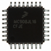
MC908JL16CFJE Freescale Semiconductor, MC908JL16CFJE Datasheet - Page 127

MC908JL16CFJE
Manufacturer Part Number
MC908JL16CFJE
Description
IC MCU 16K FLASH 8MHZ 32-LQFP
Manufacturer
Freescale Semiconductor
Series
HC08r
Datasheet
1.MC908JL16CFJER.pdf
(230 pages)
Specifications of MC908JL16CFJE
Core Processor
HC08
Core Size
8-Bit
Speed
8MHz
Connectivity
I²C, SCI
Peripherals
LED, LVD, POR, PWM
Number Of I /o
26
Program Memory Size
16KB (16K x 8)
Program Memory Type
FLASH
Ram Size
512 x 8
Voltage - Supply (vcc/vdd)
2.7 V ~ 5.5 V
Data Converters
A/D 13x10b
Oscillator Type
Internal
Operating Temperature
-40°C ~ 85°C
Package / Case
32-LQFP
Processor Series
HC08JL
Core
HC08
Data Bus Width
8 bit
Data Ram Size
512 B
Interface Type
SCI
Maximum Clock Frequency
8 MHz
Number Of Programmable I/os
26
Number Of Timers
4
Operating Supply Voltage
2.7 V to 5.5 V
Maximum Operating Temperature
+ 85 C
Mounting Style
SMD/SMT
Development Tools By Supplier
FSICEBASE, DEMO908JL16E, M68CBL05CE
Minimum Operating Temperature
- 40 C
On-chip Adc
13-ch x 10-bit
Controller Family/series
HC08
No. Of I/o's
26
Ram Memory Size
512Byte
Cpu Speed
8MHz
No. Of Timers
2
Embedded Interface Type
I2C, SCI, SPI
Rohs Compliant
Yes
For Use With
DEMO908JL16E - BOARD DEMO FOR MC908JL16
Lead Free Status / RoHS Status
Lead free / RoHS Compliant
Eeprom Size
-
Lead Free Status / Rohs Status
Lead free / RoHS Compliant
Available stocks
Company
Part Number
Manufacturer
Quantity
Price
Company:
Part Number:
MC908JL16CFJE
Manufacturer:
Freescale Semiconductor
Quantity:
1 806
Company:
Part Number:
MC908JL16CFJE
Manufacturer:
Freescale Semiconductor
Quantity:
10 000
Part Number:
MC908JL16CFJE
Manufacturer:
FREESCALE
Quantity:
20 000
Company:
Part Number:
MC908JL16CFJER
Manufacturer:
Freescale Semiconductor
Quantity:
29 890
Company:
Part Number:
MC908JL16CFJER
Manufacturer:
Freescale
Quantity:
198
Company:
Part Number:
MC908JL16CFJER
Manufacturer:
Freescale Semiconductor
Quantity:
10 000
The maximum total conversion time for a single conversion or the first conversion in continuous
conversion mode is determined by the clock source chosen and the divide ratio selected. The clock
source is selectable by the ADICLK and ACLKEN bits, and the divide ratio is specified by the ADIV bits.
For example, if the alternate clock source is 16 MHz and is selected as the input clock source, the input
clock divide-by-8 ratio is selected and the bus frequency is 4 MHz, then the conversion time for a single
10-bit conversion is:
9.3.4 Sources of Error
Several sources of error exist for ADC conversions. These are discussed in the following sections.
9.3.4.1 Sampling Error
For proper conversions, the input must be sampled long enough to achieve the proper accuracy. Given
the maximum input resistance of approximately 15 kΩ and input capacitance of approximately 10 pF,
sampling to within
1/4
maximum ADCK frequency) provided the resistance of the external analog source (R
kΩ. Higher source resistances or higher-accuracy sampling is possible by setting ADLSMP (to increase
the sample window to 23.5 cycles) or decreasing ADCK frequency to increase sample time.
9.3.4.2 Pin Leakage Error
Leakage on the I/O pins can cause conversion error if the external analog source resistance (R
If this error cannot be tolerated by the application, keep R
1/4
9.3.4.3 Noise-Induced Errors
System noise which occurs during the sample or conversion process can affect the accuracy of the
conversion. The ADC10 accuracy numbers are guaranteed as specified only if the following conditions
are met:
Freescale Semiconductor
•
•
•
•
•
•
LSB
LSB
There is a 0.1µF low-ESR capacitor from V
There is a 0.1µF low-ESR capacitor from V
If inductive isolation is used from the primary supply, an additional 1µF capacitor is placed from
V
V
The MCU is placed in wait mode immediately after initiating the conversion (next instruction after
write to ADCSC).
There is no I/O switching, input or output, on the MCU during the conversion.
(at 10-bit resolution) can be achieved within the minimum sample window (3.5 cycles / 2 MHz
leakage error (at 10-bit resolution).
DDA
SSA
Maximum Conversion time =
and V
to V
The ADCK frequency must be between f
maximum to meet A/D specifications.
SSA
REFL
(if available).
(if available) is connected to V
Number of bus cycles = 11.25 µs x 4 MHz = 45 cycles
MC68HC908JL16 Data Sheet, Rev. 1.1
21 ADCK cycles
16 MHz/8
NOTE
REFH
DDA
SS
to V
ADCK
to V
AS
at a quiet point in the ground plane.
SSA
lower than V
REFL
+
minimum and f
(if available).
3 bus cycles
(if available).
4 MHz
ADVIN
ADCK
/ (4096*I
= 11.25 µs
Functional Description
AS
Leak
) is kept below 10
) for less than
AS
) is high.
127


