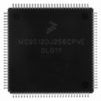
MC9S12DJ256CPVE Freescale Semiconductor, MC9S12DJ256CPVE Datasheet - Page 17

MC9S12DJ256CPVE
Manufacturer Part Number
MC9S12DJ256CPVE
Description
IC MCU 256K FLASH 4K EE 112-LQFP
Manufacturer
Freescale Semiconductor
Series
HCS12r
Specifications of MC9S12DJ256CPVE
Core Processor
HCS12
Core Size
16-Bit
Speed
25MHz
Connectivity
CAN, I²C, SCI, SPI
Peripherals
PWM, WDT
Number Of I /o
91
Program Memory Size
256KB (256K x 8)
Program Memory Type
FLASH
Eeprom Size
4K x 8
Ram Size
12K x 8
Voltage - Supply (vcc/vdd)
2.35 V ~ 5.25 V
Data Converters
A/D 16x10b
Oscillator Type
Internal
Operating Temperature
-40°C ~ 85°C
Package / Case
112-LQFP
Processor Series
S12D
Core
HCS12
Data Bus Width
16 bit
Data Ram Size
12 KB
Interface Type
CAN/I2C/SCI/SPI
Maximum Clock Frequency
25 MHz
Number Of Programmable I/os
59
Number Of Timers
8
Operating Supply Voltage
- 0.3 V to + 6 V
Maximum Operating Temperature
+ 85 C
Mounting Style
SMD/SMT
3rd Party Development Tools
EWHCS12
Development Tools By Supplier
M68KIT912DP256
Minimum Operating Temperature
- 40 C
On-chip Adc
2 (8-ch x 10-bit)
Package
112LQFP
Family Name
HCS12
Maximum Speed
25 MHz
Lead Free Status / RoHS Status
Lead free / RoHS Compliant
Available stocks
Company
Part Number
Manufacturer
Quantity
Price
Company:
Part Number:
MC9S12DJ256CPVE
Manufacturer:
Freescale Semiconductor
Quantity:
10 000
Document References
The Device User Guide provides information about the MC9S12DT128B device made up of standard
HCS12 blocks and the HCS12 processor core.
This document is part of the customer documentation. A complete set of device manuals also includes the
HCS12 Core User Guide and all the individual Block User Guides of the implemented modules. In a effort
to reduce redundancy all module specific information is located only in the respective Block User Guide.
If applicable, special implementation details of the module are given in the block description sections of
this document.
See Table 0-2 for names and versions of the referenced documents throughout the Device User Guide.
Analog to Digital Converter 10 Bit 8 Channel (ATD_10B8C) Block User Guide
Enhanced Capture Timer 16 Bit 8 Channel (ECT_16B8C) Block User Guide
Pulse Width Modulator 8 Bit 8 Channel (PWM_8B8C) Block User Guide
– Port M[7:6]
– Port P6
– Port S[7:4]
– PAD[15:8] (ATD1 channels)
PM7:6 must be configured as outputs or their pull resistors must be enabled to avoid floating
inputs.
PP6 must be configured as output or its pull resistor must be enabled to avoid a floating input.
PS7:4 must be configured as outputs or their pull resistors must be enabled to avoid floating
inputs.
Out of reset the ATD1 is disabled preventing current flows in the pins. Do not modify the ATD1
registers!
Byte Level Data Link Controller -J1850 (BDLC) Block User Guide
Port Integration Module (PIM_9DT128) Block User Guide
Asynchronous Serial Interface (SCI) Block User Guide
Clock and Reset Generator (CRG) Block User Guide
Motorola Scalable CAN (MSCAN) Block User Guide
Serial Peripheral Interface (SPI) Block User Guide
2K Byte EEPROM (EETS2K) Block User Guide
128K Byte Flash (FTS128K) Block User Guide
User Guide
Voltage Regulator (VREG) Block User Guide
Freescale Semiconductor, Inc.
For More Information On This Product,
Table 0-2 Document References
Inter IC Bus (IIC) Block User Guide
Byteflight (BF) Block User Guide
HCS12_V1.5 Core User Guide
Go to: www.freescale.com
MC9S12DT128B Device User Guide — V01.09
Version
V03
V01
V02
V02
V02
V02
V01
V01
V01
V01
V02
V01
V01
V01
1.2
Document Order Number
S12ECT16B8CV1/D
S12ATD10B8CV2/D
S12PWM8B8CV1/D
S12PIMDT128V1/D
S12FTS128KV1/D
S12EETS2KV1/D
HCS12COREUG
S12MSCANV2/D
S12VREGV1/D
S12BDLCV1/D
S12CRGV3/D
S12SCIV2/D
S12SPIV2/D
S12IICV2/D
S12BFV1/D


