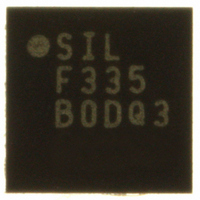
C8051F335-GM Silicon Laboratories Inc, C8051F335-GM Datasheet - Page 39

C8051F335-GM
Manufacturer Part Number
C8051F335-GM
Description
IC 8051 MCU 2KB FLASH 20QFN
Manufacturer
Silicon Laboratories Inc
Series
C8051F33xr
Specifications of C8051F335-GM
Program Memory Type
FLASH
Program Memory Size
2KB (2K x 8)
Package / Case
20-QFN
Core Processor
8051
Core Size
8-Bit
Speed
25MHz
Connectivity
SMBus (2-Wire/I²C), SPI, UART/USART
Peripherals
POR, PWM, WDT
Number Of I /o
17
Ram Size
768 x 8
Voltage - Supply (vcc/vdd)
2.7 V ~ 3.6 V
Oscillator Type
Internal
Operating Temperature
-40°C ~ 85°C
Processor Series
C8051F3x
Core
8051
Data Bus Width
8 bit
Data Ram Size
768 B
Interface Type
I2C, SPI, UART
Maximum Clock Frequency
25 MHz
Number Of Programmable I/os
17
Number Of Timers
4
Operating Supply Voltage
2.7 V to 3.6 V
Maximum Operating Temperature
+ 85 C
Mounting Style
SMD/SMT
3rd Party Development Tools
KSK-SL-TOOLSTICK, PK51, CA51, A51, ULINK2
Development Tools By Supplier
C8051F330DK
Minimum Operating Temperature
- 40 C
On-chip Adc
10 bit
No. Of I/o's
17
Ram Memory Size
768Byte
Cpu Speed
25MHz
No. Of Timers
4
Rohs Compliant
Yes
Data Rom Size
128 B
Height
0.88 mm
Length
4 mm
Supply Voltage (max)
3.6 V
Supply Voltage (min)
2.7 V
Width
4 mm
Lead Free Status / RoHS Status
Lead free / RoHS Compliant
For Use With
770-1006 - ISP 4PORT FOR SILABS C8051F MCU336-1451 - ADAPTER PROGRAM TOOLSTICK F330
Eeprom Size
-
Data Converters
-
Lead Free Status / Rohs Status
Lead free / RoHS Compliant
Other names
336-1269
- Current page: 39 of 210
- Download datasheet (2Mb)
C8051F330/1/2/3/4/5
measured from ‘0’ to VREF x 1023/1024. Example codes are shown below for both right-justified and left-
justified data. Unused bits in the ADC0H and ADC0L registers are set to ‘0’.
When in Differential Mode, conversion codes are represented as 10-bit signed 2’s complement numbers.
Inputs are measured from –VREF to VREF x 511/512. Example codes are shown below for both right-jus-
tified and left-justified data. For right-justified data, the unused MSBs of ADC0H are a sign-extension of the
data word. For left-justified data, the unused LSBs in the ADC0L register are set to ‘0’.
Important Note About ADC0 Input Configuration: Port pins selected as ADC0 inputs should be config-
ured as analog inputs, and should be skipped by the Digital Crossbar. To configure a Port pin for analog
input, set to ‘0’ the corresponding bit in register PnMDIN (for n = 0,1). To force the Crossbar to skip a Port
pin, set to ‘1’ the corresponding bit in register PnSKIP (for n = 0,1). See
on page 123
5.2.
The typical temperature sensor transfer function is shown in Figure 5.2. The output voltage (V
positive ADC input when the temperature sensor is selected by bits AMX0P4–0 in register AMX0P.
42
VREF x 1023/1024
–VREF x 256/512
VREF x 512/1024
VREF x 256/1024
VREF x 256/512
VREF x 511/512
Input Voltage
Input Voltage
Temperature Sensor
–VREF
0
0
for more Port I/O configuration details.
Right-Justified ADC0H:ADC0L
Right-Justified ADC0H:ADC0L
(AD0LJST = 0)
(AD0LJST = 0)
0x01FF
0xFF00
0xFE00
0x0100
0x0000
0x03FF
0x0200
0x0100
0x0000
Rev. 1.7
Left-Justified ADC0H:ADC0L
Left-Justified ADC0H:ADC0L
Section “14. Port Input/Output”
(AD0LJST = 1)
(AD0LJST = 1)
0x7FC0
0xFFC0
0xC000
0x4000
0x0000
0x8000
0x8000
0x4000
0x0000
TEMP
) is the
Related parts for C8051F335-GM
Image
Part Number
Description
Manufacturer
Datasheet
Request
R
Part Number:
Description:
SMD/C°/SINGLE-ENDED OUTPUT SILICON OSCILLATOR
Manufacturer:
Silicon Laboratories Inc
Part Number:
Description:
Manufacturer:
Silicon Laboratories Inc
Datasheet:
Part Number:
Description:
N/A N/A/SI4010 AES KEYFOB DEMO WITH LCD RX
Manufacturer:
Silicon Laboratories Inc
Datasheet:
Part Number:
Description:
N/A N/A/SI4010 SIMPLIFIED KEY FOB DEMO WITH LED RX
Manufacturer:
Silicon Laboratories Inc
Datasheet:
Part Number:
Description:
N/A/-40 TO 85 OC/EZLINK MODULE; F930/4432 HIGH BAND (REV E/B1)
Manufacturer:
Silicon Laboratories Inc
Part Number:
Description:
EZLink Module; F930/4432 Low Band (rev e/B1)
Manufacturer:
Silicon Laboratories Inc
Part Number:
Description:
I°/4460 10 DBM RADIO TEST CARD 434 MHZ
Manufacturer:
Silicon Laboratories Inc
Part Number:
Description:
I°/4461 14 DBM RADIO TEST CARD 868 MHZ
Manufacturer:
Silicon Laboratories Inc
Part Number:
Description:
I°/4463 20 DBM RFSWITCH RADIO TEST CARD 460 MHZ
Manufacturer:
Silicon Laboratories Inc
Part Number:
Description:
I°/4463 20 DBM RADIO TEST CARD 868 MHZ
Manufacturer:
Silicon Laboratories Inc
Part Number:
Description:
I°/4463 27 DBM RADIO TEST CARD 868 MHZ
Manufacturer:
Silicon Laboratories Inc
Part Number:
Description:
I°/4463 SKYWORKS 30 DBM RADIO TEST CARD 915 MHZ
Manufacturer:
Silicon Laboratories Inc
Part Number:
Description:
N/A N/A/-40 TO 85 OC/4463 RFMD 30 DBM RADIO TEST CARD 915 MHZ
Manufacturer:
Silicon Laboratories Inc
Part Number:
Description:
I°/4463 20 DBM RADIO TEST CARD 169 MHZ
Manufacturer:
Silicon Laboratories Inc


