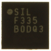
C8051F335-GM Silicon Laboratories Inc, C8051F335-GM Datasheet - Page 82

C8051F335-GM
Manufacturer Part Number
C8051F335-GM
Description
IC 8051 MCU 2KB FLASH 20QFN
Manufacturer
Silicon Laboratories Inc
Series
C8051F33xr
Specifications of C8051F335-GM
Program Memory Type
FLASH
Program Memory Size
2KB (2K x 8)
Package / Case
20-QFN
Core Processor
8051
Core Size
8-Bit
Speed
25MHz
Connectivity
SMBus (2-Wire/I²C), SPI, UART/USART
Peripherals
POR, PWM, WDT
Number Of I /o
17
Ram Size
768 x 8
Voltage - Supply (vcc/vdd)
2.7 V ~ 3.6 V
Oscillator Type
Internal
Operating Temperature
-40°C ~ 85°C
Processor Series
C8051F3x
Core
8051
Data Bus Width
8 bit
Data Ram Size
768 B
Interface Type
I2C, SPI, UART
Maximum Clock Frequency
25 MHz
Number Of Programmable I/os
17
Number Of Timers
4
Operating Supply Voltage
2.7 V to 3.6 V
Maximum Operating Temperature
+ 85 C
Mounting Style
SMD/SMT
3rd Party Development Tools
KSK-SL-TOOLSTICK, PK51, CA51, A51, ULINK2
Development Tools By Supplier
C8051F330DK
Minimum Operating Temperature
- 40 C
On-chip Adc
10 bit
No. Of I/o's
17
Ram Memory Size
768Byte
Cpu Speed
25MHz
No. Of Timers
4
Rohs Compliant
Yes
Data Rom Size
128 B
Height
0.88 mm
Length
4 mm
Supply Voltage (max)
3.6 V
Supply Voltage (min)
2.7 V
Width
4 mm
Lead Free Status / RoHS Status
Lead free / RoHS Compliant
For Use With
770-1006 - ISP 4PORT FOR SILABS C8051F MCU336-1451 - ADAPTER PROGRAM TOOLSTICK F330
Eeprom Size
-
Data Converters
-
Lead Free Status / Rohs Status
Lead free / RoHS Compliant
Other names
336-1269
9.3.
The CIP-51 includes an extended interrupt system supporting a total of 13 interrupt sources with two prior-
ity levels. The allocation of interrupt sources between on-chip peripherals and external inputs pins varies
according to the specific version of the device. Each interrupt source has one or more associated interrupt-
pending flag(s) located in an SFR. When a peripheral or external source meets a valid interrupt condition,
the associated interrupt-pending flag is set to logic 1.
If interrupts are enabled for the source, an interrupt request is generated when the interrupt-pending flag is
set. As soon as execution of the current instruction is complete, the CPU generates an LCALL to a prede-
termined address to begin execution of an interrupt service routine (ISR). Each ISR must end with an RETI
instruction, which returns program execution to the next instruction that would have been executed if the
interrupt request had not occurred. If interrupts are not enabled, the interrupt-pending flag is ignored by the
hardware and program execution continues as normal. (The interrupt-pending flag is set to logic 1 regard-
less of the interrupt's enable/disable state.)
Each interrupt source can be individually enabled or disabled through the use of an associated interrupt
enable bit in an SFR (IE–EIE1). However, interrupts must first be globally enabled by setting the EA bit
(IE.7) to logic 1 before the individual interrupt enables are recognized. Setting the EA bit to logic 0 disables
all interrupt sources regardless of the individual interrupt-enable settings.
Note: Any instruction that clears the EA bit should be immediately followed by an instruction that has two
or more opcode bytes. For example:
// in 'C':
EA = 0; // clear EA bit.
Bits7–0: ACC: Accumulator.
Bits7–0: B: B Register.
ACC.7
R/W
R/W
B.7
Bit7
Bit7
Interrupt Handler
This register is the accumulator for arithmetic operations.
This register serves as a second accumulator for certain arithmetic operations.
ACC.6
R/W
R/W
B.6
Bit6
Bit6
ACC.5
SFR Definition 9.5. ACC: Accumulator
R/W
R/W
B.5
Bit5
Bit5
SFR Definition 9.6. B: B Register
ACC.4
R/W
R/W
B.4
Bit4
Bit4
Rev. 1.7
ACC.3
R/W
R/W
B.3
Bit3
Bit3
ACC.2
R/W
R/W
Bit2
B.2
Bit2
C8051F330/1/2/3/4/5
ACC.1
R/W
R/W
B.1
Bit1
Bit1
(bit addressable)
(bit addressable)
ACC.0
R/W
R/W
B.0
Bit0
Bit0
SFR Address:
SFR Address:
00000000
00000000
Reset Value
Reset Value
0xE0
0xF0
85


