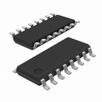
C8051F829-GS Silicon Laboratories Inc, C8051F829-GS Datasheet - Page 116

C8051F829-GS
Manufacturer Part Number
C8051F829-GS
Description
IC MCU 8BIT 8KB FLASH 16SOIC
Manufacturer
Silicon Laboratories Inc
Series
C8051F82xr
Datasheet
1.C8051F800DK.pdf
(250 pages)
Specifications of C8051F829-GS
Core Processor
8051
Core Size
8-Bit
Speed
25MHz
Connectivity
SMBus (2-Wire/I²C), SPI, UART/USART
Peripherals
POR, PWM, WDT
Number Of I /o
13
Program Memory Size
8KB (8K x 8)
Program Memory Type
FLASH
Ram Size
256 x 8
Voltage - Supply (vcc/vdd)
1.8 V ~ 3.6 V
Oscillator Type
Internal
Operating Temperature
-40°C ~ 85°C
Package / Case
16-SOIC (3.9mm Width)
Processor Series
C8051F8x
Core
8051
Data Bus Width
16 bit
Data Ram Size
256 B
Interface Type
I2C, SPI, UART
Maximum Clock Frequency
25 MHz
Number Of Programmable I/os
13
Number Of Timers
3
Operating Supply Voltage
1.8 V to 3.6 V
Maximum Operating Temperature
+ 125 C
Mounting Style
SMD/SMT
3rd Party Development Tools
PK51, CA51, A51, ULINK2
Development Tools By Supplier
C8051F800DK
Minimum Operating Temperature
- 55 C
Lead Free Status / RoHS Status
Lead free / RoHS Compliant
Eeprom Size
-
Data Converters
-
Lead Free Status / Rohs Status
Details
Other names
336-1809-5
Available stocks
Company
Part Number
Manufacturer
Quantity
Price
Company:
Part Number:
C8051F829-GS
Manufacturer:
Silicon Laboratories Inc
Quantity:
135
C8051F80x-83x
the VDD Monitor or the VDD Monitor reset source is not enabled, a Flash Error Device Reset will be
generated when the firmware attempts to modify the Flash.
The following guidelines are recommended for any system that contains routines which write or erase
Flash from code.
19.4.1. VDD Maintenance and the VDD Monitor
1. If the system power supply is subject to voltage or current "spikes," add sufficient transient protection
2. Make certain that the minimum VDD rise time specification of 1 ms is met. If the system cannot meet
3. Keep the on-chip VDD Monitor enabled and enable the VDD Monitor as a reset source as early in code
Note: On C8051F80x-83x devices, both the VDD Monitor and the VDD Monitor reset source must be enabled to write
4. As an added precaution, explicitly enable the VDD Monitor and enable the VDD Monitor as a reset
5. Make certain that all writes to the RSTSRC (Reset Sources) register use direct assignment operators
6. Make certain that all writes to the RSTSRC register explicitly set the PORSF bit to a 1. Areas to check
19.4.2. PSWE Maintenance
1. Reduce the number of places in code where the PSWE bit (b0 in PSCTL) is set to a 1. There should be
2. Minimize the number of variable accesses while PSWE is set to a 1. Handle pointer address updates
3. Disable interrupts prior to setting PSWE to a 1 and leave them disabled until after PSWE has been
4. Make certain that the Flash write and erase pointer variables are not located in XRAM. See your
116
devices to the power supply to ensure that the supply voltages listed in the Absolute Maximum Ratings
table are not exceeded.
this rise time specification, then add an external VDD brownout circuit to the RST pin of the device that
holds the device in reset until VDD reaches the minimum device operating voltage and re-asserts RST
if VDD drops below the minimum device operating voltage.
as possible. This should be the first set of instructions executed after the Reset Vector. For C-based
systems, this will involve modifying the startup code added by the C compiler. See your compiler
documentation for more details. Make certain that there are no delays in software between enabling the
VDD Monitor and enabling the VDD Monitor as a reset source. Code examples showing this can be
found in “AN201: Writing to Flash from Firmware," available from the Silicon Laboratories website.
source inside the functions that write and erase Flash memory. The VDD Monitor enable instructions
should be placed just after the instruction to set PSWE to a 1, but before the Flash write or erase
operation instruction.
and explicitly DO NOT use the bit-wise operators (such as AND or OR). For example, "RSTSRC =
0x02" is correct, but "RSTSRC |= 0x02" is incorrect.
are initialization code which enables other reset sources, such as the Missing Clock Detector or
Comparator, for example, and instructions which force a Software Reset. A global search on "RSTSRC"
can quickly verify this.
exactly one routine in code that sets PSWE to a 1 to write Flash bytes and one routine in code that sets
both PSWE and PSEE both to a 1 to erase Flash pages.
and loop maintenance outside the "PSWE = 1;... PSWE = 0;" area. Code examples showing this can be
found in “AN201: Writing to Flash from Firmware," available from the Silicon Laboratories website.
reset to 0. Any interrupts posted during the Flash write or erase operation will be serviced in priority
order after the Flash operation has been completed and interrupts have been re-enabled by software.
compiler documentation for instructions regarding how to explicitly locate variables in different memory
areas.
or erase Flash without generating a Flash Error Device Reset.
On C8051F80x-83x devices, both the VDD Monitor and the VDD Monitor reset source are enabled by hardware
after a power-on reset.
Rev. 1.0


