DSP56F826BU80E Freescale Semiconductor, DSP56F826BU80E Datasheet
DSP56F826BU80E
Specifications of DSP56F826BU80E
Available stocks


Related parts for DSP56F826BU80E


DSP56F826BU80E Summary of contents
Page 1
Data Sheet Preliminary Technical Data 56F800 16-bit Digital Signal Controllers DSP56F826 Rev. 14 01/2007 freescale.com ...
Page 2
...
Page 3
... SPI1 Applica- or GPIO tion-Specific 4 Memory & Dedicated GPIO Peripherals 16 Freescale Semiconductor • One Serial Port Interface (SPI) • One additional SPI or two optional Serial Communication Interfaces (SCI) • One Synchronous Serial Interface (SSI) • One General Purpose Quad Timer • JTAG/OnCE • ...
Page 4
... One Serial Peripheral Interface with 4 pins (or four additional GPIO lines) • One Serial Peripheral Interface, or multiplexed with two Serial Communications Interfaces totalling 4 pins • Synchronous Serial Interface (SSI) with configurable six-pin port (or six additional GPIO lines) 4 Data memory Program memory 56F826 Technical Data, Rev. 14 Freescale Semiconductor ...
Page 5
... Program and Data Flash memory areas. Both Program and Data Flash memories can be independently bulk-erased or erased in page sizes of 256 words. The Boot Flash memory can also be either bulk- or page-erased. Freescale Semiconductor 56F826 Technical Data, Rev. 14 56F826 Description ...
Page 6
... Product Documentation The four documents listed in Table 1-1 56F826. Documentation is available from local Freescale distributors, Freescale Semiconductor sales offices, Freescale Literature Distribution Centers, or online at www.freescale.com. Table 1-1 56F826 Chip Documentation Topic 56800E ...
Page 7
... A high true (active high) signal is low or a low true (active low) signal is high. Examples: Signal/Symbol PIN PIN PIN PIN 1. Values for and Freescale Semiconductor Logic State True False True False are defined by individual product specifications. OH 56F826 Technical Data, Rev. 14 Data Sheet Conventions Signal State 1 Voltage Asserted ...
Page 8
... Serial Peripheral Interface (SPI) Port Serial Communications Interface (SCI) Ports Interrupt and Program Control 1. Alternately, GPIO pins 8 Table 2-1 describes the signal or signals present on a pin. Functional Group V ) DDIO or DDA V ) SSIO or SSA 56F826 Technical Data, Rev. 14 Table 2-1 Number of Pins (3,4,1) (3,4, Freescale Semiconductor ...
Page 9
... TA0 (GPIOF0) Quad Timer A TA1 (GPIOF1) or GPIO TA2 (GPIOF2) TA3 (GPIOF3) JTAG/OnCE™ Port * Includes TCS pin, which is reserved for factory use and is tied to VSS Figure 2-1 56F826 Signals Identified by Functional Group 1. Alternate pin functionality is shown in parentheses. Freescale Semiconductor DDA 1 V DDIO 4 ...
Page 10
... TCS—This pin is reserved for factory use. It must be tied block diagrams, this pin is considered an additional V External Crystal Oscillator Input—This input should be connected to a 4MHz external crystal or ceramic resonator. For more information, please refer to Section 3.6. 56F826 Technical Data, Rev. 14 for normal use. SS SS. Freescale Semiconductor ...
Page 11
... A6 16 (GPIOE6 (GPIOE7) Freescale Semiconductor Description Crystal Oscillator Output—This output connects the internal crystal oscillator output to an external crystal or ceramic resonator external clock source over 4MHz is used, XTAL must be used as the input and EXTAL connected For more information, please refer to External Clock Input— ...
Page 12
... Data Bus— D0–D15 specify the data for external program or data memory accesses. D0–D15 are tri-stated when the external bus is inactive. Program Memory Select—PS is asserted low for external program memory access. Data Memory Select—DS is asserted low for external data memory access. 56F826 Technical Data, Rev. 14 Freescale Semiconductor ...
Page 13
... Input (Schmitt Output Freescale Semiconductor Description Read Enable—RD is asserted during external memory read cycles. When RD is asserted low, pins D0–D15 become inputs and an external device is enabled onto the device data bus. When RD is deasserted high, the external data is latched inside the device. When RD is asserted, it qualifies the A0–A15, PS, and DS pins. RD can be connected directly to the OE pin of a Static RAM or ROM. Write Enable— ...
Page 14
... It is used to synchronize data transfer and can be an input or an output. Port C GPIO—This is a General Purpose I/O (GPIO) pin with the capability of being individually programmed as input or output. After reset, the default state is GPIO input. 56F826 Technical Data, Rev. 14 Freescale Semiconductor ...
Page 15
... Input/Output (GPIOF5) Input/Output Freescale Semiconductor Description SSI Serial Receive Clock (SRCK)—This bidirectional pin provides the serial bit rate clock for the Receive section of the SSI. The clock signal can be continuous or gated and can be used by both the transmitter and receiver in synchronous mode. Port C GPIO— ...
Page 16
... After reset, the default state is SCI output. Receive Data (RXD1)— receive data input SPI Slave Select—In master mode, this pin is used to arbitrate multiple masters. In slave mode, this pin is used to select the slave. After reset, the default state is SCI input. 56F826 Technical Data, Rev. 14 Freescale Semiconductor ...
Page 17
... Input (Schmitt) EXTBOOT 25 Input (Schmitt) Freescale Semiconductor Description External Interrupt Request A—The IRQA input is a synchronized external interrupt request that indicates that an external device is requesting service. It can be programmed to be level-sensitive or negative-edge-triggered. If level-sensitive triggering is selected, an external pull-up resistor is required for wired-OR operation. ...
Page 18
... Reliability of operation is enhanced if unused inputs are tied to an appropriate voltage level. 18 Table 3-1 are stress ratings only, and functional operation at the CAUTION normal precautions are 56F826 Technical Data, Rev. 14 advised to avoid Freescale Semiconductor ...
Page 19
... V and V must not differ by more that 0.5V DDIO DDA Table 3-2 Recommended Operating Conditions Characteristic Supply voltage, core Supply Voltage, IO and analog Voltage difference DD_IO Voltage difference _IO Ambient operating temperature Freescale Semiconductor Symbol DDIO V DDA INA , V ΔV DDA ΔV ...
Page 20
... useful value to use to estimate junction JT 56F826 Technical Data, Rev Value Unit 100-pin LQFP 48.3 °C/W 43.9 °C/W 40.7 °C/W 38.6 °C/W 13.5 °C/W 1.0 °C/W User Determined I/O θ W ( Freescale Semiconductor Notes 2 2 1.2 1 ...
Page 21
... Input current high (analog inputs, V Input current low (analog inputs, V Output High Voltage (at IOH) Output Low Voltage (at IOL) Output source current Output sink current 3 PWM pin output source current 4 PWM pin output sink current Freescale Semiconductor = 0V =3.0–3.6V 2.25–2.75V, T SSA DDA DDIO DD Symbol ...
Page 22
... EIO 2.0 2.2 2.4 EIC — 1.7 2 interrupt is generated. Functionality EIO and the point when DDIO , an interrupt is generated. Functionality of EIC and the point when the DD . While power is ramping up, this signal remains Freescale Semiconductor = 80MHz Unit ...
Page 23
... Notes rising before DDIO DDA rising much faster than V DDIO DDA Figure 3-2 Supply Voltage Sequencing and Separation Cautions Freescale Semiconductor Supply Voltage Sequencing and Separation Cautions IDD Analog IDD Total 20 40 Freq. (MHz) and 56F826 Technical Data, Rev Table ...
Page 24
... IL IH for an input signal are shown in Pulse Width Low – 56F826 Technical Data, Rev. 14 Figure 3-3. This keeps V and V DDIO DD regulator begins proper DDIO, DDA V DD levels specified in the DC Characteristics Figure 3-4. High 90% 50% 10% Rise Time and Freescale Semiconductor DD from DD reaches ...
Page 25
... Defines program cycle 6. Defines erase cycle 7. Defines mass erase cycle, erase whole block 8. Defines non-volatile store cycle Mode Read Word program Page erase Mass erase Freescale Semiconductor Data2 Valid Data2 Tri-stated Figure 3-5 Signal States Table 3-5 Flash Memory Truth Table ...
Page 26
... Figure 3-6, Figure 3-7, Figure 3-8 – us Figure 3-6, Figure 3-7 – us Figure 3-8 – us Figure 3-6 – us Figure 3-6, Figure 3-7, Figure 3-8 – ms Figure 3-6 – Figure 3-6 – Figure 3-6 – Figure 3-6 Freescale Semiconductor ...
Page 27
... YADR YE DIN PROG Tnvs NVSTR Tpgs IFREN XADR XE YE=SE=OE=MAS1=0 ERASE Tnvs NVSTR Freescale Semiconductor Tadh Tads Tprog Thv Figure 3-6 Flash Program Cycle Terase Figure 3-7 Flash Erase Cycle 56F826 Technical Data, Rev. 14 Flash Memory Characteristics Tpgh Tnvh Trcv Tnvh Trcv ...
Page 28
... EXTAL) of 10pF to 13pF over temperature and process variations. Using a typical value of internal capacitance on these pins of 12pF and a value of 3pF 28 Tme Figure 3-8 Flash Mass Erase Cycle Table 3-9. A recommended crystal oscillator circuit 56F826 Technical Data, Rev. 14 Tnvh1 Trcv Figure 3-9, no Freescale Semiconductor ...
Page 29
... XTAL pins. The internal 56F82x oscillator circuitry is designed to have no external load capacitors present. As shown in Figure 3-10, no external load capacitors should be used. EXTAL XTAL Figure 3-10 Connecting a Ceramic Resonator Note: Freescale recommends only two terminal ceramic resonators vs. three terminal resonators (which contain an internal bypass capacitor to ground). Freescale Semiconductor 9pF Recommended External Crystal Parameters: R ...
Page 30
... T SSA DDA DDIO DD Symbol Min 1 f osc t 6. – Figure 3-12 External Clock Timing 56F826 Technical Data, Rev. 14 Figure 3-11. The external clock /2. ≤ 50pF –40° to +85° Typ Max — — 90% 50% 10% Freescale Semiconductor = 80MHz Unit MHz ...
Page 31
... Data Out Hold Time from WR Deasserted Data Out Set Up Time to WR Deasserted Wait states = 0 Wait states > Deasserted to Address Not Valid Address Valid to RD Deasserted Wait states = 0 Wait states > 0 Freescale Semiconductor Table 3-9 PLL Timing = 0V 3.0–3.6V 2.25–2.75V, T SSA DDA ...
Page 32
... WRRD t RDRD t WRWR t RDWR 56F826 Technical Data, Rev (Continued) ≤ 50pF –40° to +85° 80MHz Unit Min Max 0 — — ns — ns — — (T*WS -4.4 — ns — 2.4 ns — (T*WS) + 2.4 ns 6.8 — — ns 14.1 — ns 12.8 — ns Freescale Semiconductor ...
Page 33
... A0–A15, PS, DS (See Note AWR t WRWR WR t WRD D0–D15 Note: During read-modify-write instructions and internal instructions, the address lines do not change state. Figure 3-13 External Bus Asynchronous Timing Freescale Semiconductor t ARDD t ARDA t WRRD DOS DOH Data Out 56F826 Technical Data, Rev. 14 ...
Page 34
... Figure 3-14 1.5T — ns Figure 3-15 15T — ns Figure 3-16 16T — ns Figure 3-16 13T — ns Figure 3-17 2T — ns Figure 3-18 Figure 3-18 — 275,000T ns — 12T ns Figure 3-19 — 275,000T ns — 12T ns Figure 3-19 — 275,000T ns — 12T ns Freescale Semiconductor = 80MHz op ...
Page 35
... IRQA, IRQB General Purpose I/O Pin t IG IRQA, IRQB Figure 3-16 External Level-Sensitive Interrupt Timing Freescale Semiconductor Reset, Stop, Wait, Mode Select, and Interrupt Timing IRW First Interrupt Instruction Execution a) First Interrupt Instruction Execution b) General Purpose I/O 56F826 Technical Data, Rev. 14 ...
Page 36
... IRQA A0–A15 PS, DS, RD, WR Figure 3-19 Recovery from Stop State Using IRQA Interrupt Service 36 t IRI IRQ t II 56F826 Technical Data, Rev. 14 First Interrupt Vector Instruction Fetch First Instruction Fetch Not IRQA Interrupt Vector First IRQA Interrupt Instruction Fetch Freescale Semiconductor ...
Page 37
... Slave Data Valid for outputs Master Slave (after enable edge) Data invalid Master Slave Rise time Master Slave Fall time Master Slave 1. Parameters are guaranteed by design. Freescale Semiconductor Table 3-12 SPI Timing = 0V =3.0–3.6V 2.25–2.75V, T SSA DDA DDIO DD Symbol ELD ...
Page 38
... Figure 3-21 SPI Master Timing (CPHA = held High on master MSB in Bits 14– Master MSB out Bits 14– held High on master MSB in Bits 14– Master MSB out Bits 14– 56F826 Technical Data, Rev LSB in t (ref Master LSB out LSB Master LSB out t R Freescale Semiconductor ...
Page 39
... SCLK (CPOL = 1) (Input) MISO (Output MOSI (Input) Figure 3-22 SPI Slave Timing (CPHA = 0) SS (Input) SCLK (CPOL = 0) (Input) SCLK (CPOL = 1) (Input MISO (Output) t MOSI (Input) Figure 3-23 SPI Slave Timing (CPHA = 1) Freescale Semiconductor ELD Slave MSB out Bits 14– MSB in Bits 14–1 ...
Page 40
... TFSWLM -0.1 — 0 RFSBLM -0.1 — 0 RFSWLM t 20 — 22 TXEM t 24 — 26 TXVM t 0.1 — 0.2 TXNVM t 24 — 25.5 TXHIM t 4 — — — — — — TSM t 4 — — THM Freescale Semiconductor = 80MHz Units MHz ...
Page 41
... SCKH STCK output STFS (bl) output t TFSWHM STFS (wl) output t TXVM t STXD SRCK output t RFSBHM SRFS (bl) output t RFSWHM SRFS (wl) output t SM SRXD Figure 3-24 Master Mode Timing Diagram Freescale Semiconductor t SCKW t SCKL t t TFSBHM TFSBLM t TXEM TXNVM First Bit t RFBLM t TSM THM 56F826 Technical Data, Rev. 14 ...
Page 42
... TFSBLS -1 — — TFSWLS -46 — — RFSBLS -46 — — t — — TXES t 1 — 25 TXVS t 5.5 — 25 FTXES t 6 — 27 FTXVS t 11 — 13 TXNVS t 11 — 28.5 TXHIS t 4 — — — — HS Freescale Semiconductor Units MHz ...
Page 43
... SCR2 and RFSI=0 in SCSR). If the polarity of the clock and/or the frame sync have been inverted, all the timings remain valid by inverting the clock signal STCK/SRCK and/or the frame sync STFS/SRFS in the tables and in the figures. 4. 50% duty cycle bit length word length Freescale Semiconductor 1 Switching Characteristics = 0V 3.0– ...
Page 44
... V = 2.25–2.75V, T SSA DDA DDIO DD Symbol Min P 4T 2T+3 INHL P 2T OUT P 1T OUTHL 56F826 Technical Data, Rev TFSWLS t TXHIS Last Bit t RFSWLS 1, 2 ≤ 50pF –40° to +85° 80MHz Max Unit — ns — ns — ns — ns Freescale Semiconductor ...
Page 45
... The RXD pin in SCI0 is named RXD0 and the RXD pin in SCI1 is named RXD1. 3. The TXD pin in SCI0 is named TXD0 and the TXD pin in SCI1 is named TXD1. 4. Parameters listed are guaranteed by design. RXD SCI receive data pin (Input) Freescale Semiconductor P INHL P OUTHL Figure 3-26 Quad Timer Timing Table 3-16 SCI Timing ...
Page 46
... Table 3-17 JTAG Timing = 0V =3.0–3.6V 2.25–2.75V, T SSA DDA DDIO DD Symbol TRST )/2 56F826 Technical Data, Rev ≤ 50pF –40° to +85° 80MHz Min Max Unit DC 10 MHz 100 — — ns 0.4 — ns 1.2 — ns — 26.6 ns — 23 — — Freescale Semiconductor ...
Page 47
... TCK (Input) TDI TMS (Input) TDO (Output) TDO (Output ) TDO (Output) Figure 3-30 Test Access Port Timing Diagram TRST (Input Freescale Semiconductor t DS Input Data Valid TRST Figure 3-31 TRST Timing Diagram DE Figure 3-32 OnCE—Debug Event 56F826 Technical Data, Rev ...
Page 48
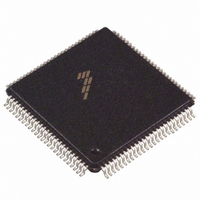
... Figure 4-1 Top View, 56F826 100-pin LQFP Package 48 ORIENTATION MARK 56F826 Technical Data, Rev. 14 GPIOD1 GPIOD0 PIN 76 GPIOB7 GPIOB6 GPIOB5 GPIOB4 GPIOB3 GPIOB2 GPIOB1 GPIOB0 CLKO XTAL EXTAL V SSA V DDA V SSIO V DDIO STCK STFS STD SRCK PIN 51 SRFS SRD Freescale Semiconductor ...
Page 49
... A13 34 10 A12 35 11 A11 36 12 A10 EXTBOOT 50 Freescale Semiconductor Signal Name Pin No. Signal Name RD 51 SRD WR 52 SRFS DS 53 SRCK PS 54 STD V 55 STFS DDIO V 56 STCK SSIO IRQA 57 V DDIO IRQB 58 V SSIO DDA SSA D2 61 EXTAL D3 62 XTAL ...
Page 50
... K 0.500 0.700 0.020 0.028 ° ° REF 12 REF N 0.090 0.160 0.004 0.006 ° ° ° 0.150 0.250 0.006 0.010 S 15.950 16.050 0.628 0.632 V 15.950 16.050 0.628 0.632 W 0.200 REF 0.008 REF X 1.000 REF 0.039 REF Freescale Semiconductor ° ...
Page 51
... This is done to minimize temperature variation across the surface. • Measure the thermal resistance from the junction to where the leads are attached to the case. This definition is approximately equal to a junction-to-board thermal resistance. Freescale Semiconductor , in °C can be obtained from the equation: J × ) ...
Page 52
... SSA layers of the PCB with approximately 100μF, preferably with a high-grade 56F826 Technical Data, Rev the temperature of the package case T V and V pin on the DD, DDIO, DDA (GND) pin. SSA V DD, DDIO, Freescale Semiconductor and ...
Page 53
... TRST should be tied low. • Because the Flash memory is programmed through the JTAG/OnCE port, designers should provide an interface to this port to allow in-circuit Flash programming. Freescale Semiconductor and V DDA 56F826 Technical Data, Rev. 14 Electrical Design Considerations pins ...
Page 54
... V 2.25-2.75 V 56F826 3.0–3.6 V 2.25-2.75 V *This package is RoHS compliant. 54 Package Type Plastic Quad Flat Pack (LQFP) Plastic Quad Flat Pack (LQFP) 56F826 Technical Data, Rev. 14 Ambient Pin Frequency Order Number Count (MHz) 100 80 DSP56F826BU80 100 80 DSP56F826BU80E * Freescale Semiconductor ...
Page 55
... Freescale Semiconductor 56F826 Technical Data, Rev. 14 Electrical Design Considerations 55 ...
Page 56
... Freescale Semiconductor was negligent regarding the design or manufacture of the part. Freescale™ and the Freescale logo are trademarks of Freescale Semiconductor, Inc. All other product or service names are the property of their respective owners. This product incorporates SuperFlash® ...