MC68332GCEH20 Freescale Semiconductor, MC68332GCEH20 Datasheet - Page 51
MC68332GCEH20
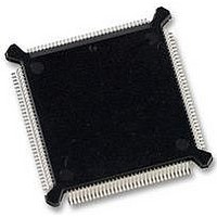
Manufacturer Part Number
MC68332GCEH20
Description
IC MCU 32BIT 20MHZ 132-PQFP
Manufacturer
Freescale Semiconductor
Series
M683xxr
Specifications of MC68332GCEH20
Core Processor
CPU32
Core Size
32-Bit
Speed
20MHz
Connectivity
EBI/EMI, SCI, SPI, UART/USART
Peripherals
POR, PWM, WDT
Number Of I /o
15
Program Memory Type
ROMless
Ram Size
2K x 8
Voltage - Supply (vcc/vdd)
4.5 V ~ 5.5 V
Oscillator Type
Internal
Operating Temperature
-40°C ~ 85°C
Package / Case
132-QFP
Controller Family/series
68K
No. Of I/o's
15
Ram Memory Size
2KB
Cpu Speed
20MHz
No. Of Timers
1
Embedded Interface Type
QSPI, SCI, UART
Digital Ic Case Style
PQFP
Rohs Compliant
Yes
Data Bus Width
32 bit
Data Ram Size
2 KB
Interface Type
QSPI, SCI, UART
Maximum Clock Frequency
20 MHz
Number Of Programmable I/os
15
Number Of Timers
16
Maximum Operating Temperature
+ 85 C
Mounting Style
SMD/SMT
Minimum Operating Temperature
- 40 C
Lead Free Status / RoHS Status
Lead free / RoHS Compliant
Eeprom Size
-
Program Memory Size
-
Data Converters
-
Lead Free Status / Rohs Status
Details
Available stocks
Company
Part Number
Manufacturer
Quantity
Price
Company:

Part Number:
MC68332GCEH20
Manufacturer:
Freescale Semiconductor
Quantity:
10 000
Part Number:
MC68332GCEH20
Manufacturer:
FREESCALE
Quantity:
20 000


4.7 Background Debugging Mode
MC68332
MC68332TS/D
The background debugger on the CPU32 is implemented in CPU microcode. The background debug-
ging commands are summarized below.
Read Memory Location
Write Memory Location
Read System Register
Write System Register
Dump Memory Block
Resume Execution
Read D/A Register
Write D/A Register
Reset Peripherals
Fill Memory Block
Patch User Code
No Operation
Command
Freescale Semiconductor, Inc.
WDREG/WAREG The data operand is written to the specified address or data
RDREG/RAREG
For More Information On This Product,
Mnemonic
Table 21 Background Debuggung Mode
WSREG
RSREG
WRITE
DUMP
READ
CALL
NOP
FILL
RST
GO
Go to: www.freescale.com
Read the selected address or data register and return the
results through the serial interface.
register.
The specified system control register is read. All registers that
can be read in supervisor mode can be read in background
mode.
The operand data is written into the specified system control
register.
Read the sized data at the memory location specified by the
long-word address. The source function code register (SFC)
determines the address space accessed.
Write the operand data to the memory location specified by the
long-word address. The destination function code (DFC)
register determines the address space accessed.
Used in conjunction with the READ command to dump large
blocks of memory. An initial READ is executed to set up the
starting address of the block and retrieve the first result.
Subsequent operands are retrieved with the DUMP command.
Used in conjunction with the WRITE command to fill large
blocks of memory. Initially, a WRITE is executed to set up the
starting address of the block and supply the first operand. The
FILL command writes subsequent operands.
The pipe is flushed and refilled before resuming instruction
execution at the current PC.
Current program counter is stacked at the location of the
current stack pointer. Instruction execution begins at user
patch code.
Asserts RESET for 512 clock cycles. The CPU is not reset by
this command. Synonymous with the CPU RESET instruction.
NOP performs no operation and can be used as a null
command.
Description
MOTOROLA
51
Related parts for MC68332GCEH20
Image
Part Number
Description
Manufacturer
Datasheet
Request
R

Part Number:
Description:
Manufacturer:
Freescale Semiconductor, Inc
Datasheet:
Part Number:
Description:
Manufacturer:
Freescale Semiconductor, Inc
Datasheet:
Part Number:
Description:
Manufacturer:
Freescale Semiconductor, Inc
Datasheet:
Part Number:
Description:
Manufacturer:
Freescale Semiconductor, Inc
Datasheet:
Part Number:
Description:
Manufacturer:
Freescale Semiconductor, Inc
Datasheet:
Part Number:
Description:
Manufacturer:
Freescale Semiconductor, Inc
Datasheet:
Part Number:
Description:
Manufacturer:
Freescale Semiconductor, Inc
Datasheet:
Part Number:
Description:
Manufacturer:
Freescale Semiconductor, Inc
Datasheet:
Part Number:
Description:
Manufacturer:
Freescale Semiconductor, Inc
Datasheet:
Part Number:
Description:
Manufacturer:
Freescale Semiconductor, Inc
Datasheet:
Part Number:
Description:
Manufacturer:
Freescale Semiconductor, Inc
Datasheet:
Part Number:
Description:
Manufacturer:
Freescale Semiconductor, Inc
Datasheet:
Part Number:
Description:
Manufacturer:
Freescale Semiconductor, Inc
Datasheet:
Part Number:
Description:
Manufacturer:
Freescale Semiconductor, Inc
Datasheet:
Part Number:
Description:
Manufacturer:
Freescale Semiconductor, Inc
Datasheet: