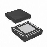
ATTINY48-MMU Atmel, ATTINY48-MMU Datasheet - Page 15

ATTINY48-MMU
Manufacturer Part Number
ATTINY48-MMU
Description
MCU AVR 5K FLASH 12MHZ 28-QFN
Manufacturer
Atmel
Series
AVR® ATtinyr
Specifications of ATTINY48-MMU
Core Processor
AVR
Core Size
8-Bit
Speed
12MHz
Connectivity
I²C, SPI
Peripherals
Brown-out Detect/Reset, POR, WDT
Number Of I /o
24
Program Memory Size
4KB (2K x 16)
Program Memory Type
FLASH
Eeprom Size
64 x 8
Ram Size
256 x 8
Voltage - Supply (vcc/vdd)
1.8 V ~ 5.5 V
Data Converters
A/D 6x10b
Oscillator Type
Internal
Operating Temperature
-40°C ~ 85°C
Package / Case
28-VQFN Exposed Pad, 28-HVQFN, 28-SQFN, 28-DHVQFN
Processor Series
ATTINY4x
Core
AVR8
Data Bus Width
8 bit
Data Ram Size
256 B
Interface Type
2-Wire, I2S, SPI
Maximum Clock Frequency
12 MHz
Number Of Programmable I/os
24
Number Of Timers
2
Maximum Operating Temperature
+ 85 C
Mounting Style
SMD/SMT
3rd Party Development Tools
EWAVR, EWAVR-BL
Development Tools By Supplier
ATAVRDRAGON, ATSTK500, ATSTK600, ATAVRISP2, ATAVRONEKIT
Minimum Operating Temperature
- 40 C
On-chip Adc
10 bit, 6 Channel
Package
28VQFN EP
Device Core
AVR
Family Name
ATtiny
Maximum Speed
12 MHz
Operating Supply Voltage
2.5|3.3|5 V
For Use With
ATAVRDRAGON - KIT DRAGON 32KB FLASH MEM AVR
Lead Free Status / RoHS Status
Lead free / RoHS Compliant
- Current page: 15 of 302
- Download datasheet (9Mb)
4.9
4.9.1
4.9.2
8008G–AVR–04/11
Register Description
SPH and SPL — Stack Pointer Registers
SREG – Status Register
• Bits 9:0 – SP[10:0]: Stack Pointer
The Stack Pointer register points to the top of the stack, which is implemented growing from
higher memory locations to lower memory locations. Hence, a stack PUSH command decreases
the Stack Pointer.
The stack space in the data SRAM must be defined by the program before any subroutine calls
are executed or interrupts are enabled.
• Bit 7 – I: Global Interrupt Enable
The Global Interrupt Enable bit must be set for the interrupts to be enabled. The individual inter-
rupt enable control is then performed in separate control registers. If the Global Interrupt Enable
Register is cleared, none of the interrupts are enabled independent of the individual interrupt
enable settings. The I-bit is cleared by hardware after an interrupt has occurred, and is set by
the RETI instruction to enable subsequent interrupts. The I-bit can also be set and cleared by
the application with the SEI and CLI instructions, as described in the instruction set reference.
• Bit 6 – T: Bit Copy Storage
The Bit Copy instructions BLD (Bit LoaD) and BST (Bit STore) use the T-bit as source or desti-
nation for the operated bit. A bit from a register in the Register File can be copied into T by the
BST instruction, and a bit in T can be copied into a bit in a register in the Register File by the
BLD instruction.
• Bit 5 – H: Half Carry Flag
The Half Carry Flag H indicates a Half Carry in some arithmetic operations. Half Carry Is useful
in BCD arithmetic. See the “Instruction Set Description” for detailed information.
• Bit 4 – S: Sign Bit, S = N
The S-bit is always an exclusive or between the Negative Flag N and the Two’s Complement
Overflow Flag V. See the “Instruction Set Description” for detailed information.
Initial Value
Read/Write
Bit
0x3E (0x5E)
0x3D (0x5D)
Bit
Read/Write
Initial Value
Bit
0x3F (0x5F)
Read/Write
Initial Value
RAMEND
R/W
SP7
R/W
15
7
0
I
R
0
–
7
RAMEND
R/W
SP6
R/W
14
6
T
0
R
0
–
6
⊕
V
RAMEND
R/W
SP5
R/W
H
13
5
0
R
0
–
5
RAMEND
R/W
SP4
R/W
12
S
4
0
R
0
–
4
RAMEND
R/W
SP3
R/W
11
V
3
0
R
–
3
0
RAMEND
R/W
SP2
R/W
10
N
2
0
R
2
0
–
RAMEND
RAMEND
R/W
R/W
SP9
SP1
R/W
Z
1
0
9
1
ATtiny48/88
RAMEND
RAMEND
R/W
R/W
R/W
SP8
SP0
C
0
0
8
0
SREG
SPH
SPL
15
Related parts for ATTINY48-MMU
Image
Part Number
Description
Manufacturer
Datasheet
Request
R

Part Number:
Description:
Manufacturer:
Atmel Corporation
Datasheet:

Part Number:
Description:
MCU AVR 4K ISP FLASH 1.8V 32TQFP
Manufacturer:
Atmel
Datasheet:

Part Number:
Description:
MCU AVR 4K ISP FLASH 1.8V 32-QFN
Manufacturer:
Atmel
Datasheet:

Part Number:
Description:
MCU AVR 4K ISP FLASH 1.8V 28-DIP
Manufacturer:
Atmel
Datasheet:

Part Number:
Description:
MCU AVR 4KB FLASH 12MHZ 32TQFP
Manufacturer:
Atmel
Datasheet:

Part Number:
Description:
MCU AVR 4KB FLASH 12MHZ 32QFN
Manufacturer:
Atmel
Datasheet:

Part Number:
Description:
MCU AVR 4KB FLASH 12MHZ 28-VQFN
Manufacturer:
Atmel
Datasheet:

Part Number:
Description:
MCU AVR 4KB FLASH 12MHZ 28QFN
Manufacturer:
Atmel
Datasheet:

Part Number:
Description:
8-bit Microcontrollers - MCU 4KB FL,64B EE, 256B SRAM-12MHz
Manufacturer:
Atmel

Part Number:
Description:
8-bit Microcontrollers - MCU Microcontroller
Manufacturer:
Atmel

Part Number:
Description:
Manufacturer:
Atmel Corporation
Datasheet:


