PIC16LF1826-I/MV Microchip Technology, PIC16LF1826-I/MV Datasheet - Page 329
PIC16LF1826-I/MV
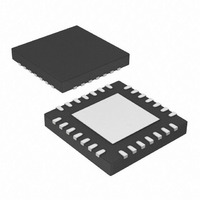
Manufacturer Part Number
PIC16LF1826-I/MV
Description
IC MCU 8BIT FLASH 28UQFN
Manufacturer
Microchip Technology
Series
PIC® XLP™ 16Fr
Datasheet
1.PIC16F1826-IP.pdf
(406 pages)
Specifications of PIC16LF1826-I/MV
Core Size
8-Bit
Program Memory Size
3.5KB (2K x 14)
Core Processor
PIC
Speed
32MHz
Connectivity
I²C, SPI, UART/USART
Peripherals
Brown-out Detect/Reset, POR, PWM, WDT
Number Of I /o
16
Program Memory Type
FLASH
Eeprom Size
256 x 8
Ram Size
256 x 8
Voltage - Supply (vcc/vdd)
1.8 V ~ 3.6 V
Data Converters
A/D 12x10b
Oscillator Type
Internal
Operating Temperature
-40°C ~ 85°C
Package / Case
28-UFQFN Exposed Pad
Controller Family/series
PIC16LF
No. Of I/o's
16
Eeprom Memory Size
256Byte
Ram Memory Size
256Byte
Cpu Speed
32MHz
No. Of Timers
3
Processor Series
PIC16LF
Core
PIC
Data Ram Size
256 B
Maximum Clock Frequency
32 KHz
Number Of Programmable I/os
16
Number Of Timers
3
Operating Supply Voltage
1.8 V to 3.6 V
Maximum Operating Temperature
+ 125 C
3rd Party Development Tools
52715-96, 52716-328, 52717-734
Development Tools By Supplier
PG164130, DV164035, DV244005, DV164005
Minimum Operating Temperature
- 40 C
On-chip Adc
10 bit, 12 Channel
On-chip Dac
5 bit
Lead Free Status / RoHS Status
Lead free / RoHS Compliant
Lead Free Status / RoHS Status
Lead free / RoHS Compliant


28.0
Each PIC16 instruction is a 14-bit word containing the
operation code (opcode) and all required operands.
The opcodes are broken into three broad categories.
• Byte Oriented
• Bit Oriented
• Literal and Control
The literal and control category contains the most var-
ied instruction word format.
Table 28-3 lists the instructions recognized by the
MPASM
All instructions are executed within a single instruction
cycle, with the following exceptions, which may take
two or three cycles:
• Subroutine takes two cycles (CALL, CALLW)
• Returns from interrupts or subroutines take two
• Program branching takes two cycles (GOTO, BRA,
• One additional instruction cycle will be used when
One instruction cycle consists of 4 oscillator cycles; for
an oscillator frequency of 4 MHz, this gives a nominal
instruction execution rate of 1 MHz.
All instruction examples use the format ‘0xhh’ to
represent a hexadecimal number, where ‘h’ signifies a
hexadecimal digit.
2010 Microchip Technology Inc.
cycles (RETURN, RETLW, RETFIE)
BRW, BTFSS, BTFSC, DECFSZ, INCSFZ)
any instruction references an indirect file register
and the file select register is pointing to program
memory.
TM
INSTRUCTION SET SUMMARY
assembler.
Preliminary
28.1
Any instruction that specifies a file register as part of
the instruction performs a Read-Modify-Write (R-M-W)
operation. The register is read, the data is modified,
and the result is stored according to either the instruc-
tion, or the destination designator ‘d’. A read operation
is performed on a register even if the instruction writes
to that register.
TABLE 28-1:
TABLE 28-2:
Field
Field
mm
DC
PC
TO
PD
W
C
b
d
n
Z
k
x
f
PIC16F/LF1826/27
Register file address (0x00 to 0x7F)
Working register (accumulator)
Bit address within an 8-bit file register
Literal field, constant data or label
Don’t care location (= 0 or 1).
The assembler will generate code with x = 0.
It is the recommended form of use for
compatibility with all Microchip software tools.
Destination select; d = 0: store result in
d = 1: store result in file register f.
Default is d = 1.
FSR or INDF number. (0-1)
Pre-post increment-decrement mode
selection
Program Counter
Time-out bit
Carry bit
Digit carry bit
Zero bit
Power-down bit
Read-Modify-Write Operations
OPCODE FIELD
DESCRIPTIONS
ABBREVIATION
DESCRIPTIONS
Description
Description
DS41391C-page 329
W
,
Related parts for PIC16LF1826-I/MV
Image
Part Number
Description
Manufacturer
Datasheet
Request
R

Part Number:
Description:
IC, 8BIT MCU, PIC16LF, 32MHZ, QFN-28
Manufacturer:
Microchip Technology
Datasheet:

Part Number:
Description:
IC, 8BIT MCU, PIC16LF, 32MHZ, QFN-28
Manufacturer:
Microchip Technology
Datasheet:

Part Number:
Description:
IC, 8BIT MCU, PIC16LF, 32MHZ, DIP-18
Manufacturer:
Microchip Technology
Datasheet:

Part Number:
Description:
IC, 8BIT MCU, PIC16LF, 20MHZ, TQFP-44
Manufacturer:
Microchip Technology
Datasheet:
Part Number:
Description:
7 KB Flash, 384 Bytes RAM, 32 MHz Int. Osc, 16 I/0, Enhanced Mid Range Core, Nan
Manufacturer:
Microchip Technology

Part Number:
Description:
14KB Flash, 512B RAM, LCD, 11x10b ADC, EUSART, NanoWatt XLP 28 SOIC .300in T/R
Manufacturer:
Microchip Technology
Datasheet:
Part Number:
Description:
14KB Flash, 512B RAM, LCD, 11x10b ADC, EUSART, NanoWatt XLP 28 SSOP .209in T/R
Manufacturer:
Microchip Technology
Datasheet:
Part Number:
Description:
MCU PIC 14KB FLASH XLP 28-SSOP
Manufacturer:
Microchip Technology
Part Number:
Description:
MCU PIC 14KB FLASH XLP 28-SOIC
Manufacturer:
Microchip Technology
Part Number:
Description:
MCU PIC 512B FLASH XLP 28-UQFN
Manufacturer:
Microchip Technology
Part Number:
Description:
MCU PIC 14KB FLASH XLP 28-SPDIP
Manufacturer:
Microchip Technology

Part Number:
Description:
MCU 7KB FLASH 256B RAM 40-UQFN
Manufacturer:
Microchip Technology
Part Number:
Description:
MCU 7KB FLASH 256B RAM 44-TQFP
Manufacturer:
Microchip Technology

Part Number:
Description:
MCU 14KB FLASH 1KB RAM 28-UQFN
Manufacturer:
Microchip Technology
Part Number:
Description:
MCU PIC 14KB FLASH XLP 40-UQFN
Manufacturer:
Microchip Technology