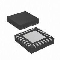
ATMEGA168PA-MMH Atmel, ATMEGA168PA-MMH Datasheet - Page 90

ATMEGA168PA-MMH
Manufacturer Part Number
ATMEGA168PA-MMH
Description
MCU AVR 16KB FLASH 28-VQFN
Manufacturer
Atmel
Series
AVR® ATmegar
Specifications of ATMEGA168PA-MMH
Core Processor
AVR
Core Size
8-Bit
Speed
20MHz
Connectivity
I²C, SPI, UART/USART
Peripherals
Brown-out Detect/Reset, POR, PWM, WDT
Number Of I /o
23
Program Memory Size
16KB (8K x 16)
Program Memory Type
FLASH
Eeprom Size
512 x 8
Ram Size
1K x 8
Voltage - Supply (vcc/vdd)
1.8 V ~ 5.5 V
Data Converters
A/D 8x10b
Oscillator Type
Internal
Operating Temperature
-40°C ~ 85°C
Package / Case
28-VQFN Exposed Pad, 28-HVQFN, 28-SQFN, 28-DHVQFN
For Use With
ATSTK600-TQFP32 - STK600 SOCKET/ADAPTER 32-TQFPATAVRDRAGON - KIT DRAGON 32KB FLASH MEM AVR
Lead Free Status / RoHS Status
Lead free / RoHS Compliant
Available stocks
Company
Part Number
Manufacturer
Quantity
Price
Part Number:
ATMEGA168PA-MMH
Manufacturer:
ATMEL/爱特梅尔
Quantity:
20 000
- Current page: 90 of 566
- Download datasheet (23Mb)
ATmega48A/48PA/88A/88PA/168A/168PA/328/328
The alternate pin configuration is as follows:
• AIN1/OC2B/PCINT23 – Port D, Bit 7
AIN1, Analog Comparator Negative Input. Configure the port pin as input with the internal pull-up
switched off to avoid the digital port function from interfering with the function of the Analog
Comparator.
PCINT23: Pin Change Interrupt source 23. The PD7 pin can serve as an external interrupt
source.
• AIN0/OC0A/PCINT22 – Port D, Bit 6
AIN0, Analog Comparator Positive Input. Configure the port pin as input with the internal pull-up
switched off to avoid the digital port function from interfering with the function of the Analog
Comparator.
OC0A, Output Compare Match output: The PD6 pin can serve as an external output for the
Timer/Counter0 Compare Match A. The PD6 pin has to be configured as an output (DDD6 set
(one)) to serve this function. The OC0A pin is also the output pin for the PWM mode timer
function.
PCINT22: Pin Change Interrupt source 22. The PD6 pin can serve as an external interrupt
source.
• T1/OC0B/PCINT21 – Port D, Bit 5
T1, Timer/Counter1 counter source.
OC0B, Output Compare Match output: The PD5 pin can serve as an external output for the
Timer/Counter0 Compare Match B. The PD5 pin has to be configured as an output (DDD5 set
(one)) to serve this function. The OC0B pin is also the output pin for the PWM mode timer
function.
PCINT21: Pin Change Interrupt source 21. The PD5 pin can serve as an external interrupt
source.
• XCK/T0/PCINT20 – Port D, Bit 4
XCK, USART external clock.
T0, Timer/Counter0 counter source.
PCINT20: Pin Change Interrupt source 20. The PD4 pin can serve as an external interrupt
source.
• INT1/OC2B/PCINT19 – Port D, Bit 3
INT1, External Interrupt source 1: The PD3 pin can serve as an external interrupt source.
OC2B, Output Compare Match output: The PD3 pin can serve as an external output for the
Timer/Counter0 Compare Match B. The PD3 pin has to be configured as an output (DDD3 set
(one)) to serve this function. The OC2B pin is also the output pin for the PWM mode timer
function.
PCINT19: Pin Change Interrupt source 19. The PD3 pin can serve as an external interrupt
source.
90
8271C–AVR–08/10
Related parts for ATMEGA168PA-MMH
Image
Part Number
Description
Manufacturer
Datasheet
Request
R

Part Number:
Description:
Manufacturer:
Atmel Corporation
Datasheet:

Part Number:
Description:
Manufacturer:
Atmel Corporation
Datasheet:

Part Number:
Description:
Manufacturer:
ATMEL Corporation
Datasheet:

Part Number:
Description:
IC AVR MCU 16K 20MHZ 32TQFP
Manufacturer:
Atmel
Datasheet:

Part Number:
Description:
IC AVR MCU 16K 20MHZ 32-QFN
Manufacturer:
Atmel
Datasheet:

Part Number:
Description:
IC AVR MCU 16K 20MHZ 28DIP
Manufacturer:
Atmel
Datasheet:

Part Number:
Description:
MCU AVR 16K FLASH 15MHZ 32-TQFP
Manufacturer:
Atmel
Datasheet:

Part Number:
Description:
MCU AVR 16K FLASH 15MHZ 32-QFN
Manufacturer:
Atmel
Datasheet:

Part Number:
Description:
IC AVR MCU 16K 20MHZ 32TQFP
Manufacturer:
Atmel
Datasheet:

Part Number:
Description:
MCU AVR 16KB FLASH 20MHZ 32QFN
Manufacturer:
Atmel
Datasheet:

Part Number:
Description:
MCU AVR 16KB FLASH 20MHZ 32TQFP
Manufacturer:
Atmel
Datasheet:

Part Number:
Description:
IC MCU AVR 16K FLASH 32-QFN
Manufacturer:
Atmel
Datasheet:


