PIC18LF13K22-I/ML Microchip Technology, PIC18LF13K22-I/ML Datasheet - Page 12
PIC18LF13K22-I/ML
Manufacturer Part Number
PIC18LF13K22-I/ML
Description
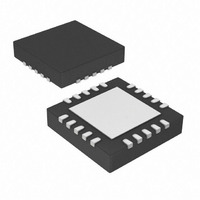
IC PIC MCU FLASH 256KX8 20-QFN
Manufacturer
Microchip Technology
Series
PIC® XLP™ 18Fr
Datasheets
1.PIC18LF13K22-ISS.pdf
(388 pages)
2.PIC18LF13K22-ISS.pdf
(12 pages)
3.PIC18LF13K22-ISS.pdf
(36 pages)
4.PIC18LF14K22-IP.pdf
(382 pages)
Specifications of PIC18LF13K22-I/ML
Program Memory Type
FLASH
Program Memory Size
8KB (4K x 16)
Package / Case
20-VQFN Exposed Pad, 20-HVQFN, 20-SQFN, 20-DHVQFN
Core Processor
PIC
Core Size
8-Bit
Speed
64MHz
Connectivity
I²C, LIN, SPI, UART/USART
Peripherals
Brown-out Detect/Reset, POR, PWM, WDT
Number Of I /o
17
Eeprom Size
256 x 8
Ram Size
256 x 8
Voltage - Supply (vcc/vdd)
1.8 V ~ 3.6 V
Data Converters
A/D 12x10b
Oscillator Type
Internal
Operating Temperature
-40°C ~ 85°C
Processor Series
PIC18LF
Core
PIC
Data Bus Width
8 bit
Data Ram Size
256 B
Interface Type
I2C, MSSP, SPI, USART
Maximum Clock Frequency
32 KHz
Number Of Programmable I/os
18
Number Of Timers
4
Operating Supply Voltage
1.8 V to 3.6 V
Maximum Operating Temperature
+ 125 C
Mounting Style
SMD/SMT
3rd Party Development Tools
52715-96, 52716-328, 52717-734, 52712-325, EWPIC18
Development Tools By Supplier
PG164130, DV164035, DV244005, DV164005
Minimum Operating Temperature
- 40 C
On-chip Adc
10 bit, 12 Channel
Lead Free Status / RoHS Status
Lead free / RoHS Compliant
Lead Free Status / RoHS Status
Lead free / RoHS Compliant, Lead free / RoHS Compliant
Available stocks
Company
Part Number
Manufacturer
Quantity
Price
Company:

Part Number:
PIC18LF13K22-I/ML
Manufacturer:
CAVIUM
Quantity:
155


PIC18F1XK22/LF1XK22
FIGURE 4-2:
4.1.2
When using low-voltage ICSP, the part must be
supplied by the voltage specified in parameter D111 if a
Bulk Erase is to be executed. All other Bulk Erase
details as described above apply.
If it is determined that a program memory erase must
be performed at a supply voltage below the Bulk Erase
limit, refer to the erase methodology described in
Section 4.1.3 “ICSP Row Erase” and Section 4.2.1
“Modifying Program Flash”.
If it is determined that a data EEPROM erase must be
performed at a supply voltage below the Bulk Erase
limit, follow the methodology described in Section 4.3
“Data EEPROM Programming” and write ‘1’s to the
array.
DS41357B-page 12
PGC
PGD
4-bit Command
1
0
LOW-VOLTAGE ICSP BULK ERASE
2
0
3
1
4
1
P5
BULK ERASE TIMING DIAGRAM
1
1
Data Payload
2
1
16-bit
15 16
0
0
P5A
4-bit Command
1
0
Advance Information
2
0
3
0
PGD = Input
4
0
P5
1
0
Data Payload
2
0
16-bit
4.1.3
Regardless of whether high or low-voltage ICSP is
used, it is possible to erase one row (64 bytes of data),
provided the block is not code or write-protected. Rows
are located at static boundaries beginning at program
memory address 000000h, extending to the internal
program memory limit (see Section 3.0 “Memory
Maps”).
The Row Erase duration is self-timed. After the WR bit
in EECON1 is set, two NOPs are issued. Erase starts
upon the 4th PGC of the second NOP. It ends when the
WR bit is cleared by hardware.
The code sequence to Row Erase a PIC18F1XK22/
LF1XK22 device is shown in Table 4-3. The flowchart
shown in Figure 4-3 depicts the logic necessary to com-
pletely erase the PIC18F1XK22/LF1XK22 devices. The
timing diagram for Row Erase is identical to the data
EEPROM write timing shown in Figure 4-7.
15 16
0
Note 1: The TBLPTR register can point at any
0
P5A
2: ICSP row erase of the User ID locations
4-bit Command
1
ICSP ROW ERASE
0
byte within the row intended for erase.
is also possible using the technique
described in Section 4.1.3 “ICSP Row
Erase”. The address argument used
should be 0x200000. A row erase of the
User ID locations is required when V
below the Bulk Erase threshold.
2
0
3
0
4
0
© 2009 Microchip Technology Inc.
Erase Time
P11
P10
Data Payload
16-bit
1
n
2
n
DD
is
Related parts for PIC18LF13K22-I/ML
Image
Part Number
Description
Manufacturer
Datasheet
Request
R

Part Number:
Description:
Manufacturer:
Microchip Technology Inc.
Datasheet:
Part Number:
Description:
Manufacturer:
Microchip Technology Inc.
Datasheet:
Part Number:
Description:
Manufacturer:
Microchip Technology Inc.
Datasheet:
Part Number:
Description:
Manufacturer:
Microchip Technology Inc.
Datasheet:
Part Number:
Description:
Manufacturer:
Microchip Technology Inc.
Datasheet:
Part Number:
Description:
Manufacturer:
Microchip Technology Inc.
Datasheet:
Part Number:
Description:
Manufacturer:
Microchip Technology Inc.
Datasheet:
Part Number:
Description:
Manufacturer:
Microchip Technology Inc.
Datasheet: