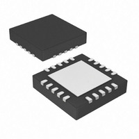
PIC18LF13K22-I/ML Microchip Technology, PIC18LF13K22-I/ML Datasheet - Page 24

PIC18LF13K22-I/ML
Manufacturer Part Number
PIC18LF13K22-I/ML
Description
IC PIC MCU FLASH 256KX8 20-QFN
Manufacturer
Microchip Technology
Series
PIC® XLP™ 18Fr
Datasheets
1.PIC18LF13K22-ISS.pdf
(388 pages)
2.PIC18LF13K22-ISS.pdf
(12 pages)
3.PIC18LF13K22-ISS.pdf
(36 pages)
4.PIC18LF14K22-IP.pdf
(382 pages)
Specifications of PIC18LF13K22-I/ML
Program Memory Type
FLASH
Program Memory Size
8KB (4K x 16)
Package / Case
20-VQFN Exposed Pad, 20-HVQFN, 20-SQFN, 20-DHVQFN
Core Processor
PIC
Core Size
8-Bit
Speed
64MHz
Connectivity
I²C, LIN, SPI, UART/USART
Peripherals
Brown-out Detect/Reset, POR, PWM, WDT
Number Of I /o
17
Eeprom Size
256 x 8
Ram Size
256 x 8
Voltage - Supply (vcc/vdd)
1.8 V ~ 3.6 V
Data Converters
A/D 12x10b
Oscillator Type
Internal
Operating Temperature
-40°C ~ 85°C
Processor Series
PIC18LF
Core
PIC
Data Bus Width
8 bit
Data Ram Size
256 B
Interface Type
I2C, MSSP, SPI, USART
Maximum Clock Frequency
32 KHz
Number Of Programmable I/os
18
Number Of Timers
4
Operating Supply Voltage
1.8 V to 3.6 V
Maximum Operating Temperature
+ 125 C
Mounting Style
SMD/SMT
3rd Party Development Tools
52715-96, 52716-328, 52717-734, 52712-325, EWPIC18
Development Tools By Supplier
PG164130, DV164035, DV244005, DV164005
Minimum Operating Temperature
- 40 C
On-chip Adc
10 bit, 12 Channel
Lead Free Status / RoHS Status
Lead free / RoHS Compliant
Lead Free Status / RoHS Status
Lead free / RoHS Compliant, Lead free / RoHS Compliant
Available stocks
Company
Part Number
Manufacturer
Quantity
Price
Company:
Part Number:
PIC18LF13K22-I/ML
Manufacturer:
CAVIUM
Quantity:
155
PIC18F1XK22/LF1XK22
5.3
A Configuration address may be read and output on
PGD via the 4-bit command, ‘1001’. Configuration data
is read and written in a byte-wise fashion, so it is not
necessary to merge two bytes into a word prior to a
compare. The result may then be immediately
compared to the appropriate configuration data in the
programmer’s memory for verification. Refer to
Section 5.1 “Read Program Flash, ID Locations and
Configuration Bits” for implementation details of
reading Configuration data.
5.4
Data EEPROM is accessed one byte at a time via an
Address Pointer (register EEADR) and a data latch
(EEDATA). Data EEPROM is read by loading EEADR
with the desired memory location and initiating a
memory
EECON1 register. The data will be loaded into
EEDATA, where it may be serially output on PGD via
the 4-bit command, ‘0010’ (Shift Out Data Holding
register). A delay of P6 must be introduced after the
falling edge of the 8th PGC of the operand to allow
PGD to transition from an input to an output. During this
time, PGC must be held low (see Figure 5-4).
The command sequence to read a single byte of data
is shown in Table 5-2.
TABLE 5-2:
DS41357B-page 24
Step 1: Direct access to data EEPROM.
Step 2: Set the data EEPROM Address Pointer.
Step 3: Initiate a memory read.
Step 4: Load data into the Serial Data Holding register.
Note 1:
Command
0000
0000
0000
0000
0000
0000
0000
0000
0010
4-bit
Verify Configuration Bits
Read Data EEPROM Memory
read
The <LSB> is undefined. The <MSB> is the data.
by
READ DATA EEPROM MEMORY
appropriately
<MSB><LSB>
Data Payload
0E <Addr>
9E A6
9C A6
6E A9
80 A6
50 A8
6E F5
00 00
configuring
BCF EECON1, EEPGD
BCF EECON1, CFGS
MOVLW <Addr>
MOVWF EEADR
BSF EECON1, RD
MOVF EEDATA, W, 0
MOVWF TABLAT
NOP
Shift Out Data
Advance Information
the
(1)
FIGURE 5-3:
Core Instruction
No
Move to TABLAT
READ DATA EEPROM
FLOW
Shift Out Data
© 2009 Microchip Technology Inc.
Address
done?
Read
Byte
Start
Done
Set
Yes


