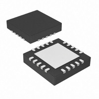
PIC18LF13K22-I/ML Microchip Technology, PIC18LF13K22-I/ML Datasheet - Page 18

PIC18LF13K22-I/ML
Manufacturer Part Number
PIC18LF13K22-I/ML
Description
IC PIC MCU FLASH 256KX8 20-QFN
Manufacturer
Microchip Technology
Series
PIC® XLP™ 18Fr
Datasheets
1.PIC18LF13K22-ISS.pdf
(388 pages)
2.PIC18LF13K22-ISS.pdf
(12 pages)
3.PIC18LF13K22-ISS.pdf
(36 pages)
4.PIC18LF14K22-IP.pdf
(382 pages)
Specifications of PIC18LF13K22-I/ML
Program Memory Type
FLASH
Program Memory Size
8KB (4K x 16)
Package / Case
20-VQFN Exposed Pad, 20-HVQFN, 20-SQFN, 20-DHVQFN
Core Processor
PIC
Core Size
8-Bit
Speed
64MHz
Connectivity
I²C, LIN, SPI, UART/USART
Peripherals
Brown-out Detect/Reset, POR, PWM, WDT
Number Of I /o
17
Eeprom Size
256 x 8
Ram Size
256 x 8
Voltage - Supply (vcc/vdd)
1.8 V ~ 3.6 V
Data Converters
A/D 12x10b
Oscillator Type
Internal
Operating Temperature
-40°C ~ 85°C
Processor Series
PIC18LF
Core
PIC
Data Bus Width
8 bit
Data Ram Size
256 B
Interface Type
I2C, MSSP, SPI, USART
Maximum Clock Frequency
32 KHz
Number Of Programmable I/os
18
Number Of Timers
4
Operating Supply Voltage
1.8 V to 3.6 V
Maximum Operating Temperature
+ 125 C
Mounting Style
SMD/SMT
3rd Party Development Tools
52715-96, 52716-328, 52717-734, 52712-325, EWPIC18
Development Tools By Supplier
PG164130, DV164035, DV244005, DV164005
Minimum Operating Temperature
- 40 C
On-chip Adc
10 bit, 12 Channel
Lead Free Status / RoHS Status
Lead free / RoHS Compliant
Lead Free Status / RoHS Status
Lead free / RoHS Compliant, Lead free / RoHS Compliant
Available stocks
Company
Part Number
Manufacturer
Quantity
Price
Company:
Part Number:
PIC18LF13K22-I/ML
Manufacturer:
CAVIUM
Quantity:
155
PIC18F1XK22/LF1XK22
4.3
Data EEPROM is accessed one byte at a time via an
Address Pointer (register EEADR) and a data latch
(EEDATA). Data EEPROM is written by loading
EEADR with the desired memory location, EEDATA
with the data to be written and initiating a memory write
by appropriately configuring the EECON1 register. A
byte write automatically erases the location and writes
the new data (erase-before-write).
When using the EECON1 register to perform a data
EEPROM write, both the EEPGD and CFGS bits must
be cleared (EECON1<7:6> = 00). The WREN bit must
be set (EECON1<2> = 1) to enable writes of any sort
and this must be done prior to initiating a write
sequence. The write sequence is initiated by setting the
WR bit (EECON1<1> = 1).
The write begins on the falling edge of the 24th PGC
after the WR bit is set. It ends when the WR bit is
cleared by hardware.
After the programming sequence terminates, PGC
must be held low for the time specified by parameter
P10 to allow high-voltage discharge of the memory
array.
FIGURE 4-7:
DS41357B-page 18
PGC
PGD
Poll WR bit
Data EEPROM Programming
4-bit Command
1
0
2
0
3
0
4
PGD
0
PGC
P5
DATA EEPROM WRITE TIMING DIAGRAM
BSF EECON1, WR
1
4-bit Command
2
1
0
2
0
15 16
3
0
4
0
P5A
P5
MOVF EECON1, W, 0
2 NOP commands
1
Advance Information
2
PGD = Input
PGD = Input
15 16
P5A
P5A
4-bit Command
1
0
FIGURE 4-6:
2
0
3
0
4
0
Poll WR bit, Repeat until Clear
P5
MOVWF TABLAT
1
(see below)
No
2
P11A
15 16
PROGRAM DATA FLOW
Enable Write
Set Address
Start Write
Sequence
© 2009 Microchip Technology Inc.
Set Data
done?
WR bit
clear?
Start
Done
P5A
Yes
Yes
(see Figure 4-4)
PGD = Output
Shift Out Data
No
P10
16-bit Data
Payload
1
n
2
n


