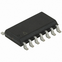
ATTINY24-15SSZ Atmel, ATTINY24-15SSZ Datasheet - Page 112

ATTINY24-15SSZ
Manufacturer Part Number
ATTINY24-15SSZ
Description
MCU AVR 2K FLASH 15MHZ 14-SOIC
Manufacturer
Atmel
Series
AVR® ATtinyr
Datasheet
1.ATTINY24-15SSZ.pdf
(225 pages)
Specifications of ATTINY24-15SSZ
Package / Case
14-SOIC (3.9mm Width), 14-SOL
Voltage - Supply (vcc/vdd)
2.7 V ~ 5.5 V
Operating Temperature
-40°C ~ 125°C
Speed
16MHz
Number Of I /o
12
Eeprom Size
128 x 8
Core Processor
AVR
Program Memory Type
FLASH
Ram Size
128 x 8
Program Memory Size
2KB (2K x 8)
Data Converters
A/D 8x10b
Oscillator Type
Internal
Peripherals
Brown-out Detect/Reset, POR, PWM, WDT
Connectivity
USI
Core Size
8-Bit
Cpu Family
ATtiny
Device Core
AVR
Device Core Size
8b
Frequency (max)
16MHz
Interface Type
SPI/UART
Total Internal Ram Size
128Byte
# I/os (max)
12
Number Of Timers - General Purpose
2
Operating Supply Voltage (typ)
3.3/5V
Operating Supply Voltage (max)
5.5V
Operating Supply Voltage (min)
2.7V
On-chip Adc
8-chx10-bit
Instruction Set Architecture
RISC
Operating Temp Range
-40C to 125C
Operating Temperature Classification
Automotive
Mounting
Surface Mount
Pin Count
14
Package Type
SOIC
Lead Free Status / RoHS Status
Lead free / RoHS Compliant
Available stocks
Company
Part Number
Manufacturer
Quantity
Price
Company:
Part Number:
ATTINY24-15SSZ
Manufacturer:
ATMEL
Quantity:
349
Part Number:
ATTINY24-15SSZ
Manufacturer:
ATTINY
Quantity:
20 000
- Current page: 112 of 225
- Download datasheet (4Mb)
14.11 Register Description
14.11.1
112
Atmel ATtiny24/44/84 [Preliminary]
TCCR1A – Timer/Counter1 Control Register A
• Bit 7:6 – COM1A1:0: Compare Output Mode for Channel A
• Bit 5:4 – COM1B1:0: Compare Output Mode for Channel B
The COM1A1:0 and COM1B1:0 control the output compare pins' (OC1A and OC1B, respec-
tively) behavior. If one or both of the COM1A1:0 bits are written to logical one, the OC1A
output overrides the normal port functionality of the I/O pin it is connected to. If one or both of
the COM1B1:0 bit are written to logical one, the OC1B output overrides the normal port func-
tionality of the I/O pin it is connected to. However, note that the data direction register (DDR)
bit corresponding to the OC1A or OC1B pin must be set in order to enable the output driver.
When OC1A or OC1B is connected to the pin, the function of the COM1x1:0 bits is dependent
on the WGM13:0 bit settings.
when the WGM13:0 bits are set to a normal or CTC mode (non-PWM).
Table 14-1.
Table 14-2 on page 112
to the fast PWM mode.
Table 14-2.
Note:
Bit
0x2F (0x4F)
Read/Write
Initial Value
COM1A1/COM1B1
COM1A1/COM1B1
1. A special case occurs when OCR1A/OCR1B equals TOP and COM1A1/COM1B1 is set. In
0
0
1
1
0
0
1
1
this case the compare match is ignored, but the set or clear is done at BOTTOM. See
PWM Mode” on page 103
COM1A1
Compare Output Mode, non-PWM
Compare Output Mode, Fast PWM
R/W
7
0
COM1A0
COM1A0/COM1B0
COM1A0/COM1B0
shows the COM1x1:0 bit functionality when the WGM13:0 bits are set
R/W
6
0
Table 14-1 on page 112
0
1
0
1
0
1
0
1
COM1B1
R/W
for more details.
5
0
COM1B0
R/W
4
0
Description
Normal port operation, OC1A/OC1B disconnected.
Toggle OC1A/OC1B on Compare Match.
Clear OC1A/OC1B on Compare Match (Set output to
low level).
Set OC1A/OC1B on Compare Match (Set output to
high level).
Description
Normal port operation, OC1A/OC1B disconnected.
WGM13=0: Normal port operation, OC1A/OC1B
disconnected.
WGM13=1: Toggle OC1A on Compare Match, OC1B
reserved.
Clear OC1A/OC1B on Compare Match, set
OC1A/OC1B at BOTTOM (non-inverting mode)
Set OC1A/OC1B on Compare Match, clear
OC1A/OC1B at BOTTOM (inverting mode)
(1)
R
3
–
0
shows the COM1x1:0 bit functionality
R
2
0
–
WGM11
R/W
1
0
WGM10
R/W
7701D–AVR–09/10
0
0
TCCR1A
“Fast
Related parts for ATTINY24-15SSZ
Image
Part Number
Description
Manufacturer
Datasheet
Request
R

Part Number:
Description:
Manufacturer:
Atmel Corporation
Datasheet:

Part Number:
Description:
Manufacturer:
Atmel Corporation
Datasheet:

Part Number:
Description:
IC MCU AVR 2K FLASH 20MHZ 20-QFN
Manufacturer:
Atmel
Datasheet:

Part Number:
Description:
IC MCU AVR 2K FLASH 20MHZ 14SOIC
Manufacturer:
Atmel
Datasheet:

Part Number:
Description:
MCU AVR 2K FLASH 15MHZ 20-QFN
Manufacturer:
Atmel
Datasheet:

Part Number:
Description:
IC MCU AVR 2K FLASH 20MHZ 14-DIP
Manufacturer:
Atmel
Datasheet:

Part Number:
Description:
MCU AVR 2KB FLASH 20MHZ 14SOIC
Manufacturer:
Atmel
Datasheet:

Part Number:
Description:
MCU AVR 2KB FLASH 20MHZ 20QFN
Manufacturer:
Atmel
Datasheet:

Part Number:
Description:
IC, MCU, 8BIT, 2K FLASH, 20SOIC
Manufacturer:
Atmel
Datasheet:

Part Number:
Description:
IC, MCU, 8BIT, 2K FLASH, 20PDIP
Manufacturer:
Atmel
Datasheet:

Part Number:
Description:
IC, MCU, 8BIT, 8K FLASH, 20PDIP
Manufacturer:
Atmel
Datasheet:

Part Number:
Description:
IC, MCU, 8BIT, 8K FLASH, 20SOIC
Manufacturer:
Atmel
Datasheet:


