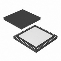
DSPIC33FJ64GS406T-I/MR Microchip Technology, DSPIC33FJ64GS406T-I/MR Datasheet - Page 403

DSPIC33FJ64GS406T-I/MR
Manufacturer Part Number
DSPIC33FJ64GS406T-I/MR
Description
MCU/DSP 16BIT 64KB FLASH 64QFN
Manufacturer
Microchip Technology
Series
dsPIC™ 33Fr
Datasheet
1.DSPIC33FJ32GS406-IPT.pdf
(418 pages)
Specifications of DSPIC33FJ64GS406T-I/MR
Program Memory Type
FLASH
Program Memory Size
64KB (64K x 8)
Package / Case
64-VQFN
Core Processor
dsPIC
Core Size
16-Bit
Speed
40 MIPs
Connectivity
I²C, IrDA, LIN, SCI, SPI, UART/USART, USB
Peripherals
Brown-out Detect/Reset, QEI, POR, PWM, WDT
Number Of I /o
58
Ram Size
8K x 8
Voltage - Supply (vcc/vdd)
3 V ~ 3.6 V
Data Converters
A/D 16x10b
Oscillator Type
Internal
Operating Temperature
-40°C ~ 85°C
Product
DSCs
Data Bus Width
16 bit
Processor Series
DSPIC33F
Core
dsPIC
Numeric And Arithmetic Format
Fixed-Point or Floating-Point
Instruction Set Architecture
Harvard
Device Million Instructions Per Second
40 MIPs
Maximum Clock Frequency
120 MHz
Number Of Programmable I/os
58
Data Ram Size
4 KB
Operating Supply Voltage
3.3 V
Maximum Operating Temperature
+ 85 C
Mounting Style
SMD/SMT
3rd Party Development Tools
52713-733, 52714-737, 53276-922, EWDSPIC
Development Tools By Supplier
PG164130, DV164035, DV244005, DV164005, PG164120, DM240001, DV164033
Interface Type
I2C, SPI, UART
Minimum Operating Temperature
- 40 C
On-chip Adc
10 bit, 16 Channel
Lead Free Status / RoHS Status
Lead free / RoHS Compliant
Eeprom Size
-
Lead Free Status / Rohs Status
Lead free / RoHS Compliant
- Current page: 403 of 418
- Download datasheet (3Mb)
APPENDIX A:
This appendix provides an overview of considerations
for migrating from the dsPIC33FJ06GS101/X02 and
dsPIC33FJ16GSX02/X04 family of devices to the
dsPIC33FJ32GS406/606/608/610
dsPIC33FJ64GS406/606/608/610 family of devices.
The code developed for the dsPIC33FJ06GS101/X02
and dsPIC33FJ16GSX02/X04 devices can be ported
to
dsPIC33FJ64GS406/606/608/610
making the appropriate changes outlined below.
A.1
On
dsPIC33FJ16GSX02/X04 devices, some peripherals
such as the Timer, Input Capture, Output Compare,
UART, SPI, External Interrupts, Analog Comparator
Output, as well as the PWM4 pin pair, were mapped to
physical pins via Peripheral Pin Select (PPS)
functionality.
and dsPIC33FJ64GS406/606/608/610 devices, these
peripherals are hard-coded to dedicated pins. Because
of this, as well as pinout differences between the two
devices families, software must be updated to utilize
peripherals on the desired pin locations.
A.2
A.2.1
Fault and Current-Limit Control Signal Source selec-
tion has changed between the two families of devices.
On
dsPIC33FJ16GSX02/X04 devices, Fault1 through
Fault8 were assigned to Fault and Current-Limit
Controls with the following values:
• 00000 = Fault 1
• 00001 = Fault 2
• 00010 = Fault 3
• 00011 = Fault 4
• 00100 = Fault 5
• 00101 = Fault 6
• 00110 = Fault 7
• 00111 = Fault 8
2010 Microchip Technology Inc.
dsPIC33FJ32GS406/606/608/610 and dsPIC33FJ64GS406/606/608/610
the
Device Pins and Peripheral Pin
Select (PPS)
High-Speed PWM
FAULT AND CURRENT-LIMIT
CONTROL SIGNAL SOURCE
SELECTION
dsPIC33FJ32GS406/606/608/610
dsPIC33FJ06GS101/X02
dsPIC33FJ06GS101/X02
On
dsPIC33FJ32GS406/606/608/610
MIGRATING FROM dsPIC33FJ06GS101/X02 AND
dsPIC33FJ16GSX02/X04 TO dsPIC33FJ32GS406/606/608/610 AND
dsPIC33FJ64GS406/606/608/610 DEVICES
devices
after
and
and
and
and
Preliminary
On
dsPIC33FJ64GS406/606/608/610
through Fault8 were assigned to Fault and Current-
Limit Controls with the following values:
• 01000 = Fault 1
• 01001 = Fault 2
• 01010 = Fault 3
• 01011 = Fault 4
• 01100 = Fault 5
• 01101 = Fault 6
• 01110 = Fault 7
• 01111 = Fault 8
A.2.2
Connection of analog comparators to the PWM Fault
and
dsPIC33FJ06GS101/X02 and dsPIC33FJ16GSX02/
X04 devices is performed by assigning a comparator to
one of the Fault sources via the virtual PPS pins, and
then selecting the desired Fault as the source for Fault
and Current-Limit Control. On dsPIC33FJ32GS406/
606/608/610 and dsPIC33FJ64GS406/606/608/610
devices, analog comparators have a direct connection
to Fault and Current-Limit Control, and can be selected
with the following values for the CLSRC or FLTSRC
bits:
• 00000 = Analog Comparator 1
• 00001 = Analog Comparator 2
• 00010 = Analog Comparator 3
• 00011 = Analog Comparator 4
A.2.3
The Leading-Edge Blanking Delay (LEB) bits have
been
dsPIC33FJ06GS101/X02 and dsPIC33FJ16GSX02/
X04
dsPIC33FJ32GS406/606/608/610
dsPIC33FJ64GS406/606/608/610 devices.
Current-Limit
devices
moved
dsPIC33FJ32GS406/606/608/610
ANALOG COMPARATORS
CONNECTION
LEADING-EDGE BLANKING (LEB)
from
to
Control
the
the
LEBDLYx
LEBCOx
Signal
DS70591C-page 403
devices,
Sources
register
register
Fault1
and
and
on
on
on
Related parts for DSPIC33FJ64GS406T-I/MR
Image
Part Number
Description
Manufacturer
Datasheet
Request
R

Part Number:
Description:
Manufacturer:
Microchip Technology Inc.
Datasheet:

Part Number:
Description:
Manufacturer:
Microchip Technology Inc.
Datasheet:

Part Number:
Description:
Manufacturer:
Microchip Technology Inc.
Datasheet:

Part Number:
Description:
Manufacturer:
Microchip Technology Inc.
Datasheet:

Part Number:
Description:
Manufacturer:
Microchip Technology Inc.
Datasheet:

Part Number:
Description:
Manufacturer:
Microchip Technology Inc.
Datasheet:

Part Number:
Description:
Manufacturer:
Microchip Technology Inc.
Datasheet:

Part Number:
Description:
Manufacturer:
Microchip Technology Inc.
Datasheet:


