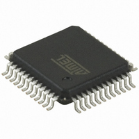
AT32UC3L064-AUT Atmel, AT32UC3L064-AUT Datasheet - Page 333

AT32UC3L064-AUT
Manufacturer Part Number
AT32UC3L064-AUT
Description
MCU AVR32 64KB FLASH 48TQFP
Manufacturer
Atmel
Series
AVR®32 UC3r
Datasheets
1.ATAVRONE-PROBECBL.pdf
(16 pages)
2.AT32UC3L-EK.pdf
(858 pages)
3.AT32UC3L016-D3HT.pdf
(110 pages)
Specifications of AT32UC3L064-AUT
Core Processor
AVR
Core Size
32-Bit
Speed
50MHz
Connectivity
I²C, SPI, UART/USART
Peripherals
Brown-out Detect/Reset, DMA, PWM, WDT
Number Of I /o
36
Program Memory Size
64KB (64K x 8)
Program Memory Type
FLASH
Ram Size
16K x 8
Voltage - Supply (vcc/vdd)
1.62 V ~ 3.6 V
Data Converters
A/D 9x10b
Oscillator Type
Internal
Operating Temperature
-40°C ~ 85°C
Package / Case
48-TQFP, 48-VQFP
Processor Series
AT32UC3x
Core
AVR32
Data Bus Width
32 bit
Data Ram Size
16 KB
Interface Type
SPI/TWI/USART
Maximum Clock Frequency
50 MHz
Number Of Programmable I/os
36
Number Of Timers
7
Maximum Operating Temperature
+ 85 C
Mounting Style
SMD/SMT
3rd Party Development Tools
EWAVR32, EWAVR32-BL
Development Tools By Supplier
AT32UC3L-EK
Minimum Operating Temperature
- 40 C
On-chip Adc
9-ch x 10-bit
Package
48TQFP
Device Core
AVR32
Family Name
AT32
Maximum Speed
50 MHz
Operating Supply Voltage
1.8|3.3 V
Lead Free Status / RoHS Status
Lead free / RoHS Compliant
Eeprom Size
-
Lead Free Status / Rohs Status
Lead free / RoHS Compliant
Available stocks
Company
Part Number
Manufacturer
Quantity
Price
Company:
Part Number:
AT32UC3L064-AUT
Manufacturer:
HONGFA
Quantity:
30 000
Part Number:
AT32UC3L064-AUT
Manufacturer:
MICROCHIP/微芯
Quantity:
20 000
- Current page: 333 of 858
- Download datasheet (13Mb)
18.7
18.7.1
32099F–11/2010
User Interface
Access Types
The GPIO controller manages all the GPIO pins on the 32-bit AVR microcontroller. The pins are
managed as 32-bit ports that are configurable through a Peripheral Bus (PB) interface. Each
port has a set of configuration registers. The overall memory map of the GPIO is shown below.
The number of pins and hence the number of ports is product specific.
Figure 18-6. Port Configuration Registers
In the peripheral muxing table in the Package and Pinout chapter each GPIO pin has a unique
number. Note that the PA, PB, PC, and PX ports do not necessarily directly correspond to the
GPIO ports. To find the corresponding port and pin the following formulas can be used:
GPIO port = floor((GPIO number) / 32), example: floor((36)/32) = 1
GPIO pin = GPIO number % 32, example: 36 % 32 = 4
Table 18-2
port address offset. The specific address of a configuration register is found by adding the regis-
ter offset and the port offset to the GPIO start address. One bit in each of the configuration
registers corresponds to a GPIO pin.
Most configuration register can be accessed in four different ways. The first address location can
be used to write the register directly. This address can also be used to read the register value.
The following addresses facilitate three different types of write access to the register. Performing
a “set” access, all bits written to one will be set. Bits written to zero will be unchanged by the
operation. Performing a “clear” access, all bits written to one will be cleared. Bits written to zero
will be unchanged by the operation. Finally, a toggle access will toggle the value of all bits writ-
shows the configuration registers for one port. Addresses shown are relative to the
Port 0 Configuration Registers
Port 1 Configuration Registers
Port 2 Configuration Registers
Port n Configuration Registers
AT32UC3L016/32/64
n*0x200
0x0000
0x0200
0x0400
333
Related parts for AT32UC3L064-AUT
Image
Part Number
Description
Manufacturer
Datasheet
Request
R

Part Number:
Description:
KIT DEV/EVAL FOR AT32UC3L0
Manufacturer:
Atmel
Datasheet:

Part Number:
Description:
KIT EVAL AVR32 UC3 MCU
Manufacturer:
Atmel
Datasheet:

Part Number:
Description:
DEV KIT FOR AVR/AVR32
Manufacturer:
Atmel
Datasheet:

Part Number:
Description:
INTERVAL AND WIPE/WASH WIPER CONTROL IC WITH DELAY
Manufacturer:
ATMEL Corporation
Datasheet:

Part Number:
Description:
Low-Voltage Voice-Switched IC for Hands-Free Operation
Manufacturer:
ATMEL Corporation
Datasheet:

Part Number:
Description:
MONOLITHIC INTEGRATED FEATUREPHONE CIRCUIT
Manufacturer:
ATMEL Corporation
Datasheet:

Part Number:
Description:
AM-FM Receiver IC U4255BM-M
Manufacturer:
ATMEL Corporation
Datasheet:

Part Number:
Description:
Monolithic Integrated Feature Phone Circuit
Manufacturer:
ATMEL Corporation
Datasheet:

Part Number:
Description:
Multistandard Video-IF and Quasi Parallel Sound Processing
Manufacturer:
ATMEL Corporation
Datasheet:

Part Number:
Description:
High-performance EE PLD
Manufacturer:
ATMEL Corporation
Datasheet:

Part Number:
Description:
8-bit Flash Microcontroller
Manufacturer:
ATMEL Corporation
Datasheet:

Part Number:
Description:
2-Wire Serial EEPROM
Manufacturer:
ATMEL Corporation
Datasheet:


