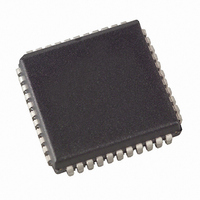
AT89C51IC2-SLSUM Atmel, AT89C51IC2-SLSUM Datasheet - Page 111

AT89C51IC2-SLSUM
Manufacturer Part Number
AT89C51IC2-SLSUM
Description
IC 8051 MCU FLASH 32K 44PLCC
Manufacturer
Atmel
Series
89Cr
Datasheet
1.AT89C51IC2-SLRIM.pdf
(147 pages)
Specifications of AT89C51IC2-SLSUM
Core Processor
8051
Core Size
8-Bit
Speed
60MHz
Connectivity
I²C, SPI, UART/USART
Peripherals
POR, PWM, WDT
Number Of I /o
34
Program Memory Size
32KB (32K x 8)
Program Memory Type
FLASH
Ram Size
1.25K x 8
Voltage - Supply (vcc/vdd)
2.7 V ~ 5.5 V
Oscillator Type
External
Operating Temperature
-40°C ~ 85°C
Package / Case
44-PLCC
Processor Series
AT89x
Core
8051
Data Bus Width
8 bit
Data Ram Size
1280 B
Interface Type
UART, SPI, TWI
Maximum Clock Frequency
60 MHz
Number Of Programmable I/os
34
Number Of Timers
3
Operating Supply Voltage
2.7 V to 5.5 V
Maximum Operating Temperature
+ 85 C
Mounting Style
SMD/SMT
3rd Party Development Tools
PK51, CA51, A51, ULINK2
Minimum Operating Temperature
- 40 C
For Use With
AT89OCD-01 - USB EMULATOR FOR AT8XC51 MCU
Lead Free Status / RoHS Status
Lead free / RoHS Compliant
Eeprom Size
-
Data Converters
-
Lead Free Status / Rohs Status
Details
Available stocks
Company
Part Number
Manufacturer
Quantity
Price
Flash Memory Status
Figure 42. Flash Memory Possible Contents
Memory Organization
4301D–8051–02/08
0000h
7FFFh
Default
Virgin
Table 88. Program Lock Bits of the SSB
Note:
AT89C51IC2 parts are delivered in standard with the ISP boot in the Flash memory.
After ISP or parallel programming, the possible contents of the Flash memory are sum-
marized on Figure 42.
In the AT89C51IC2, the lowest 32K of the 64 KB program memory address space is
filled by internal Flash.
When the EA pin is high, the processor fetches instructions from internal program Flash.
Bus expansion for accessing program memory from 32K upward automatic since exter-
nal instruction fetches occur automatically when the program counter exceeds 7FFFh
(32K). If the EA pin is tied low, all program memory fetches are from external memory.
After ISP
Security
Application
level
Program Lock Bits
1
2
3
U: unprogrammed or "one" level.
P: programmed or "zero" level.
X: don’t care
WARNING: Security level 2 and 3 should only be programmed after Flash and code
verification.
LB0
U
P
X
Dedicated
ISP
After ISP
Application
LB1
U
U
P
Virgin
or
Protection Description
No program lock features enabled.
ISP programming of the Flash is disabled.
Same as 2, also verify through ISP programming interface is disabled.
After Parallel
Programming
Application
After Parallel
Programming
Dedicated
ISP
Application
Virgin
or
111


