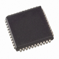
AT89C51IC2-SLSUM Atmel, AT89C51IC2-SLSUM Datasheet - Page 75

AT89C51IC2-SLSUM
Manufacturer Part Number
AT89C51IC2-SLSUM
Description
IC 8051 MCU FLASH 32K 44PLCC
Manufacturer
Atmel
Series
89Cr
Datasheet
1.AT89C51IC2-SLRIM.pdf
(147 pages)
Specifications of AT89C51IC2-SLSUM
Core Processor
8051
Core Size
8-Bit
Speed
60MHz
Connectivity
I²C, SPI, UART/USART
Peripherals
POR, PWM, WDT
Number Of I /o
34
Program Memory Size
32KB (32K x 8)
Program Memory Type
FLASH
Ram Size
1.25K x 8
Voltage - Supply (vcc/vdd)
2.7 V ~ 5.5 V
Oscillator Type
External
Operating Temperature
-40°C ~ 85°C
Package / Case
44-PLCC
Processor Series
AT89x
Core
8051
Data Bus Width
8 bit
Data Ram Size
1280 B
Interface Type
UART, SPI, TWI
Maximum Clock Frequency
60 MHz
Number Of Programmable I/os
34
Number Of Timers
3
Operating Supply Voltage
2.7 V to 5.5 V
Maximum Operating Temperature
+ 85 C
Mounting Style
SMD/SMT
3rd Party Development Tools
PK51, CA51, A51, ULINK2
Minimum Operating Temperature
- 40 C
For Use With
AT89OCD-01 - USB EMULATOR FOR AT8XC51 MCU
Lead Free Status / RoHS Status
Lead free / RoHS Compliant
Eeprom Size
-
Data Converters
-
Lead Free Status / Rohs Status
Details
Available stocks
Company
Part Number
Manufacturer
Quantity
Price
Figure 29. Data Transmission Format (CPHA = 0)
Figure 30. Data Transmission Format (CPHA = 1)
Figure 31. CPHA/SS Timing
4301D–8051–02/08
MOSI (from Master)
SCK Cycle Number
MISO (from Slave)
MOSI (from Master)
SCK (CPOL = 0)
SCK (CPOL = 1)
MISO (from Slave)
SCK Cycle Number
SPEN (Internal)
SCK (CPOL = 0)
SCK (CPOL = 1)
Capture Point
SPEN (Internal)
SS (to Slave)
Capture Point
SS (to Slave)
MISO/MOSI
(CPHA = 0)
(CPHA = 1)
Master SS
Slave SS
Slave SS
As shown in Figure 29, the first SCK edge is the MSB capture strobe. Therefore, the
Slave must begin driving its data before the first SCK edge, and a falling edge on the SS
pin is used to start the transmission. The SS pin must be toggled high and then low
between each Byte transmitted (Figure 31).
Figure 30 shows an SPI transmission in which CPHA is ’1’. In this case, the Master
begins driving its MOSI pin on the first SCK edge. Therefore, the Slave uses the first
SCK edge as a start transmission signal. The SS pin can remain low between transmis-
sions (Figure 31). This format may be preffered in systems having only one Master and
only one Slave driving the MISO data line.
MSB
MSB
MSB
1
MSB
1
2
bit6
bit6
2
bit6
Byte 1
bit6
3
bit5
bit5
3
bit5
bit5
bit4
4
bit4
bit4
4
bit4
Byte 2
bit3
bit3
5
bit3
bit3
5
6
bit2
bit2
6
bit2
bit2
Byte 3
7
bit1
bit1
7
bit1
bit1
LSB
8
LSB
LSB
8
LSB
75


