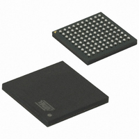
AT91SAM7X512-CU Atmel, AT91SAM7X512-CU Datasheet - Page 255

AT91SAM7X512-CU
Manufacturer Part Number
AT91SAM7X512-CU
Description
MCU ARM 512K HS FLASH 100-TFBGA
Manufacturer
Atmel
Series
AT91SAMr
Datasheet
1.AT91SAM7X512-AU-999.pdf
(687 pages)
Specifications of AT91SAM7X512-CU
Core Processor
ARM7
Core Size
16/32-Bit
Speed
55MHz
Connectivity
CAN, Ethernet, I²C, SPI, SSC, UART/USART, USB
Peripherals
Brown-out Detect/Reset, DMA, POR, PWM, WDT
Number Of I /o
62
Program Memory Size
512KB (512K x 8)
Program Memory Type
FLASH
Ram Size
128K x 8
Voltage - Supply (vcc/vdd)
1.65 V ~ 1.95 V
Data Converters
A/D 8x10b
Oscillator Type
Internal
Operating Temperature
-40°C ~ 85°C
Package / Case
100-TFBGA
Processor Series
AT91SAMx
Core
ARM7TDMI
Data Bus Width
32 bit
Data Ram Size
128 KB
Interface Type
CAN, SPI, SSC, TWI, USART, USB
Maximum Clock Frequency
55 MHz
Number Of Programmable I/os
13
Number Of Timers
3
Operating Supply Voltage
3 V to 3.6 V
Maximum Operating Temperature
+ 85 C
Mounting Style
SMD/SMT
3rd Party Development Tools
JTRACE-ARM-2M, KSK-AT91SAM7X-PL, MDK-ARM, RL-ARM, ULINK2
Development Tools By Supplier
AT91SAM-ICE, AT91-ISP, AT91SAM7X-EK
Minimum Operating Temperature
- 40 C
On-chip Adc
10 bit
Package
100TFBGA
Device Core
ARM7TDMI
Family Name
91S
Maximum Speed
55 MHz
Cpu Family
91S
Device Core Size
32b
Frequency (max)
55MHz
Total Internal Ram Size
128KB
# I/os (max)
62
Number Of Timers - General Purpose
3
Operating Supply Voltage (typ)
1.8/3.3V
Operating Supply Voltage (max)
1.95/3.6V
Operating Supply Voltage (min)
1.65/3V
Instruction Set Architecture
RISC
Operating Temp Range
-40C to 85C
Operating Temperature Classification
Industrial
Mounting
Surface Mount
Pin Count
100
Package Type
TFBGA
For Use With
AT91SAM-ICE - EMULATOR FOR AT91 ARM7/ARM9AT91SAM7X-EK - KIT EVAL FOR AT91SAM7X256/128
Lead Free Status / RoHS Status
Lead free / RoHS Compliant
Eeprom Size
-
Lead Free Status / Rohs Status
Lead free / RoHS Compliant
Available stocks
Company
Part Number
Manufacturer
Quantity
Price
- Current page: 255 of 687
- Download datasheet (11Mb)
28. Serial Peripheral Interface (SPI)
28.1
6120H–ATARM–17-Feb-09
Overview
The Serial Peripheral Interface (SPI) circuit is a synchronous serial data link that provides com-
munication with external devices in Master or Slave Mode. It also enables communication
between processors if an external processor is connected to the system.
The Serial Peripheral Interface is essentially a shift register that serially transmits data bits to
other SPIs. During a data transfer, one SPI system acts as the “master”' which controls the data
flow, while the other devices act as “slaves” which have data shifted into and out by the master.
Different CPUs can take turn being masters (Multiple Master Protocol opposite to Single Master
Protocol where one CPU is always the master while all of the others are always slaves) and one
master may simultaneously shift data into multiple slaves. However, only one slave may drive its
output to write data back to the master at any given time.
A slave device is selected when the master asserts its NSS signal. If multiple slave devices
exist, the master generates a separate slave select signal for each slave (NPCS).
The SPI system consists of two data lines and two control lines:
• Master Out Slave In (MOSI): This data line supplies the output data from the master shifted
• Master In Slave Out (MISO): This data line supplies the output data from a slave to the input
• Serial Clock (SPCK): This control line is driven by the master and regulates the flow of the
• Slave Select (NSS): This control line allows slaves to be turned on and off by hardware.
into the input(s) of the slave(s).
of the master. There may be no more than one slave transmitting data during any particular
transfer.
data bits. The master may transmit data at a variety of baud rates; the SPCK line cycles once
for each bit that is transmitted.
AT91SAM7X512/256/128 Preliminary
255
Related parts for AT91SAM7X512-CU
Image
Part Number
Description
Manufacturer
Datasheet
Request
R

Part Number:
Description:
KIT EVAL FOR AT91SAM7X256/128
Manufacturer:
Atmel
Datasheet:

Part Number:
Description:
MCU, MPU & DSP Development Tools KICKSTART KIT ATMEL AT91SAM7X
Manufacturer:
IAR Systems

Part Number:
Description:
DEV KIT FOR AVR/AVR32
Manufacturer:
Atmel
Datasheet:

Part Number:
Description:
INTERVAL AND WIPE/WASH WIPER CONTROL IC WITH DELAY
Manufacturer:
ATMEL Corporation
Datasheet:

Part Number:
Description:
Low-Voltage Voice-Switched IC for Hands-Free Operation
Manufacturer:
ATMEL Corporation
Datasheet:

Part Number:
Description:
MONOLITHIC INTEGRATED FEATUREPHONE CIRCUIT
Manufacturer:
ATMEL Corporation
Datasheet:

Part Number:
Description:
AM-FM Receiver IC U4255BM-M
Manufacturer:
ATMEL Corporation
Datasheet:

Part Number:
Description:
Monolithic Integrated Feature Phone Circuit
Manufacturer:
ATMEL Corporation
Datasheet:

Part Number:
Description:
Multistandard Video-IF and Quasi Parallel Sound Processing
Manufacturer:
ATMEL Corporation
Datasheet:

Part Number:
Description:
High-performance EE PLD
Manufacturer:
ATMEL Corporation
Datasheet:

Part Number:
Description:
8-bit Flash Microcontroller
Manufacturer:
ATMEL Corporation
Datasheet:

Part Number:
Description:
2-Wire Serial EEPROM
Manufacturer:
ATMEL Corporation
Datasheet:


