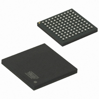
AT91SAM7X512-CU Atmel, AT91SAM7X512-CU Datasheet - Page 564

AT91SAM7X512-CU
Manufacturer Part Number
AT91SAM7X512-CU
Description
MCU ARM 512K HS FLASH 100-TFBGA
Manufacturer
Atmel
Series
AT91SAMr
Datasheet
1.AT91SAM7X512-AU-999.pdf
(687 pages)
Specifications of AT91SAM7X512-CU
Core Processor
ARM7
Core Size
16/32-Bit
Speed
55MHz
Connectivity
CAN, Ethernet, I²C, SPI, SSC, UART/USART, USB
Peripherals
Brown-out Detect/Reset, DMA, POR, PWM, WDT
Number Of I /o
62
Program Memory Size
512KB (512K x 8)
Program Memory Type
FLASH
Ram Size
128K x 8
Voltage - Supply (vcc/vdd)
1.65 V ~ 1.95 V
Data Converters
A/D 8x10b
Oscillator Type
Internal
Operating Temperature
-40°C ~ 85°C
Package / Case
100-TFBGA
Processor Series
AT91SAMx
Core
ARM7TDMI
Data Bus Width
32 bit
Data Ram Size
128 KB
Interface Type
CAN, SPI, SSC, TWI, USART, USB
Maximum Clock Frequency
55 MHz
Number Of Programmable I/os
13
Number Of Timers
3
Operating Supply Voltage
3 V to 3.6 V
Maximum Operating Temperature
+ 85 C
Mounting Style
SMD/SMT
3rd Party Development Tools
JTRACE-ARM-2M, KSK-AT91SAM7X-PL, MDK-ARM, RL-ARM, ULINK2
Development Tools By Supplier
AT91SAM-ICE, AT91-ISP, AT91SAM7X-EK
Minimum Operating Temperature
- 40 C
On-chip Adc
10 bit
Package
100TFBGA
Device Core
ARM7TDMI
Family Name
91S
Maximum Speed
55 MHz
Cpu Family
91S
Device Core Size
32b
Frequency (max)
55MHz
Total Internal Ram Size
128KB
# I/os (max)
62
Number Of Timers - General Purpose
3
Operating Supply Voltage (typ)
1.8/3.3V
Operating Supply Voltage (max)
1.95/3.6V
Operating Supply Voltage (min)
1.65/3V
Instruction Set Architecture
RISC
Operating Temp Range
-40C to 85C
Operating Temperature Classification
Industrial
Mounting
Surface Mount
Pin Count
100
Package Type
TFBGA
For Use With
AT91SAM-ICE - EMULATOR FOR AT91 ARM7/ARM9AT91SAM7X-EK - KIT EVAL FOR AT91SAM7X256/128
Lead Free Status / RoHS Status
Lead free / RoHS Compliant
Eeprom Size
-
Lead Free Status / Rohs Status
Lead free / RoHS Compliant
Available stocks
Company
Part Number
Manufacturer
Quantity
Price
- Current page: 564 of 687
- Download datasheet (11Mb)
37.3
37.3.1
564
Functional Description
AT91SAM7X512/256/128 Preliminary
Memory Interface
The EMAC has several clock domains:
The only system constraint is 160 MHz for the system bus clock, above which MDC would toggle
at above 2.5 MHz.
The system bus clock must run at least as fast as the receive clock and transmit clock (25 MHz
at 100 Mbps, and 2.5 MHz at 10 Mbps).
The control registers drive the MDIO interface, setup up DMA activity, start frame transmission
and select modes of operation such as full- or half-duplex.
The receive block checks for valid preamble, FCS, alignment and length, and presents received
frames to the address checking block and DMA interface.
The transmit block takes data from the DMA interface, adds preamble and, if necessary, pad
and FCS, and transmits data according to the CSMA/CD (carrier sense multiple access with col-
lision detect) protocol. The start of transmission is deferred if CRS (carrier sense) is active.
If COL (collision) becomes active during transmission, a jam sequence is asserted and the
transmission is retried after a random back off. CRS and COL have no effect in full duplex mode.
The DMA block connects to external memory through its ASB bus interface. It contains receive
and transmit FIFOs for buffering frame data. It loads the transmit FIFO and empties the receive
FIFO using ASB bus master operations. Receive data is not sent to memory until the address
checking logic has determined that the frame should be copied. Receive or transmit frames are
stored in one or more buffers. Receive buffers have a fixed length of 128 bytes. Transmit buffers
range in length between 0 and 2047 bytes, and up to 128 buffers are permitted per frame. The
DMA block manages the transmit and receive framebuffer queues. These queues can hold mul-
tiple frames.
Frame data is transferred to and from the EMAC through the DMA interface. All transfers are 32-
bit words and may be single accesses or bursts of 2, 3 or 4 words. Burst accesses do not cross
sixteen-byte boundaries. Bursts of 4 words are the default data transfer; single accesses or
bursts of less than four words may be used to transfer data at the beginning or the end of a
buffer.
The DMA controller performs six types of operation on the bus. In order of priority, these are:
Figure 37-1
•
•
•
1. Receive buffer manager write
2. Receive buffer manager read
3. Transmit data DMA read
4. Receive data DMA write
5. Transmit buffer manager read
6. Transmit buffer manager write
System bus clock (AHB and APB): DMA and register blocks
Transmit clock: transmit block
Receive clock: receive and address checker blocks
illustrates the different blocks of the EMAC module.
6120H–ATARM–17-Feb-09
Related parts for AT91SAM7X512-CU
Image
Part Number
Description
Manufacturer
Datasheet
Request
R

Part Number:
Description:
KIT EVAL FOR AT91SAM7X256/128
Manufacturer:
Atmel
Datasheet:

Part Number:
Description:
MCU, MPU & DSP Development Tools KICKSTART KIT ATMEL AT91SAM7X
Manufacturer:
IAR Systems

Part Number:
Description:
DEV KIT FOR AVR/AVR32
Manufacturer:
Atmel
Datasheet:

Part Number:
Description:
INTERVAL AND WIPE/WASH WIPER CONTROL IC WITH DELAY
Manufacturer:
ATMEL Corporation
Datasheet:

Part Number:
Description:
Low-Voltage Voice-Switched IC for Hands-Free Operation
Manufacturer:
ATMEL Corporation
Datasheet:

Part Number:
Description:
MONOLITHIC INTEGRATED FEATUREPHONE CIRCUIT
Manufacturer:
ATMEL Corporation
Datasheet:

Part Number:
Description:
AM-FM Receiver IC U4255BM-M
Manufacturer:
ATMEL Corporation
Datasheet:

Part Number:
Description:
Monolithic Integrated Feature Phone Circuit
Manufacturer:
ATMEL Corporation
Datasheet:

Part Number:
Description:
Multistandard Video-IF and Quasi Parallel Sound Processing
Manufacturer:
ATMEL Corporation
Datasheet:

Part Number:
Description:
High-performance EE PLD
Manufacturer:
ATMEL Corporation
Datasheet:

Part Number:
Description:
8-bit Flash Microcontroller
Manufacturer:
ATMEL Corporation
Datasheet:

Part Number:
Description:
2-Wire Serial EEPROM
Manufacturer:
ATMEL Corporation
Datasheet:


