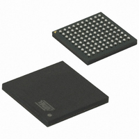
AT91SAM7X512-CU Atmel, AT91SAM7X512-CU Datasheet - Page 545

AT91SAM7X512-CU
Manufacturer Part Number
AT91SAM7X512-CU
Description
MCU ARM 512K HS FLASH 100-TFBGA
Manufacturer
Atmel
Series
AT91SAMr
Datasheet
1.AT91SAM7X512-AU-999.pdf
(687 pages)
Specifications of AT91SAM7X512-CU
Core Processor
ARM7
Core Size
16/32-Bit
Speed
55MHz
Connectivity
CAN, Ethernet, I²C, SPI, SSC, UART/USART, USB
Peripherals
Brown-out Detect/Reset, DMA, POR, PWM, WDT
Number Of I /o
62
Program Memory Size
512KB (512K x 8)
Program Memory Type
FLASH
Ram Size
128K x 8
Voltage - Supply (vcc/vdd)
1.65 V ~ 1.95 V
Data Converters
A/D 8x10b
Oscillator Type
Internal
Operating Temperature
-40°C ~ 85°C
Package / Case
100-TFBGA
Processor Series
AT91SAMx
Core
ARM7TDMI
Data Bus Width
32 bit
Data Ram Size
128 KB
Interface Type
CAN, SPI, SSC, TWI, USART, USB
Maximum Clock Frequency
55 MHz
Number Of Programmable I/os
13
Number Of Timers
3
Operating Supply Voltage
3 V to 3.6 V
Maximum Operating Temperature
+ 85 C
Mounting Style
SMD/SMT
3rd Party Development Tools
JTRACE-ARM-2M, KSK-AT91SAM7X-PL, MDK-ARM, RL-ARM, ULINK2
Development Tools By Supplier
AT91SAM-ICE, AT91-ISP, AT91SAM7X-EK
Minimum Operating Temperature
- 40 C
On-chip Adc
10 bit
Package
100TFBGA
Device Core
ARM7TDMI
Family Name
91S
Maximum Speed
55 MHz
Cpu Family
91S
Device Core Size
32b
Frequency (max)
55MHz
Total Internal Ram Size
128KB
# I/os (max)
62
Number Of Timers - General Purpose
3
Operating Supply Voltage (typ)
1.8/3.3V
Operating Supply Voltage (max)
1.95/3.6V
Operating Supply Voltage (min)
1.65/3V
Instruction Set Architecture
RISC
Operating Temp Range
-40C to 85C
Operating Temperature Classification
Industrial
Mounting
Surface Mount
Pin Count
100
Package Type
TFBGA
For Use With
AT91SAM-ICE - EMULATOR FOR AT91 ARM7/ARM9AT91SAM7X-EK - KIT EVAL FOR AT91SAM7X256/128
Lead Free Status / RoHS Status
Lead free / RoHS Compliant
Eeprom Size
-
Lead Free Status / Rohs Status
Lead free / RoHS Compliant
Available stocks
Company
Part Number
Manufacturer
Quantity
Price
- Current page: 545 of 687
- Download datasheet (11Mb)
36.8.6
Name:
Access Type:
Any modification on one of the fields of the CANBR register must be done while CAN module is disabled.
To compute the different Bit Timings, please refer to the
• PHASE2: Phase 2 segment
This phase is used to compensate the edge phase error.
Warning: PHASE2 value must be different from 0.
• PHASE1: Phase 1 segment
This phase is used to compensate for edge phase error.
• PROPAG: Programming time segment
This part of the bit time is used to compensate for the physical delay times within the network.
• SJW: Re-synchronization jump width
To compensate for phase shifts between clock oscillators of different controllers on bus. The controller must re-synchronize
on any relevant signal edge of the current transmission. The synchronization jump width defines the maximum of clock
cycles a bit period may be shortened or lengthened by re-synchronization.
• BRP: Baudrate Prescaler.
This field allows user to program the period of the CAN system clock to determine the individual bit timing.
The BRP field must be within the range [1, 0x7F], i.e., BRP = 0 is not authorized.
• SMP: Sampling Mode
0 = The incoming bit stream is sampled once at sample point.
1 = The incoming bit stream is sampled three times with a period of a MCK clock period, centered on sample point.
SMP Sampling Mode is automatically disabled if BRP = 0.
6120H–ATARM–17-Feb-09
31
23
15
–
–
–
7
–
CAN Baudrate Register
t
t
t
t
t
PHS2
PHS1
PRS
SJW
CSC
=
=
=
=
=
30
22
14
CAN_BR
Read-write
–
–
6
t
t
(
CSC
CSC
t
t
BRP
CSC
CSC
×
×
×
×
+
(
(
1
(
(
PROPAG
SJW
PHASE2
PHASE1
)
⁄
PHASE1
MCK
+
29
21
13
–
5
1
)
+
+
+
1
1
1
SJW
)
)
)
AT91SAM7X512/256/128 Preliminary
28
20
12
–
4
Section 36.6.4.1 “CAN Bit Timing Configuration” on page
BRP
27
19
11
–
–
3
–
26
18
10
–
2
PROPAG
PHASE2
25
17
–
9
1
SMP
24
16
8
0
512.
545
Related parts for AT91SAM7X512-CU
Image
Part Number
Description
Manufacturer
Datasheet
Request
R

Part Number:
Description:
KIT EVAL FOR AT91SAM7X256/128
Manufacturer:
Atmel
Datasheet:

Part Number:
Description:
MCU, MPU & DSP Development Tools KICKSTART KIT ATMEL AT91SAM7X
Manufacturer:
IAR Systems

Part Number:
Description:
DEV KIT FOR AVR/AVR32
Manufacturer:
Atmel
Datasheet:

Part Number:
Description:
INTERVAL AND WIPE/WASH WIPER CONTROL IC WITH DELAY
Manufacturer:
ATMEL Corporation
Datasheet:

Part Number:
Description:
Low-Voltage Voice-Switched IC for Hands-Free Operation
Manufacturer:
ATMEL Corporation
Datasheet:

Part Number:
Description:
MONOLITHIC INTEGRATED FEATUREPHONE CIRCUIT
Manufacturer:
ATMEL Corporation
Datasheet:

Part Number:
Description:
AM-FM Receiver IC U4255BM-M
Manufacturer:
ATMEL Corporation
Datasheet:

Part Number:
Description:
Monolithic Integrated Feature Phone Circuit
Manufacturer:
ATMEL Corporation
Datasheet:

Part Number:
Description:
Multistandard Video-IF and Quasi Parallel Sound Processing
Manufacturer:
ATMEL Corporation
Datasheet:

Part Number:
Description:
High-performance EE PLD
Manufacturer:
ATMEL Corporation
Datasheet:

Part Number:
Description:
8-bit Flash Microcontroller
Manufacturer:
ATMEL Corporation
Datasheet:

Part Number:
Description:
2-Wire Serial EEPROM
Manufacturer:
ATMEL Corporation
Datasheet:


