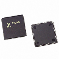
Z8F4822VS020SG Zilog, Z8F4822VS020SG Datasheet - Page 166

Z8F4822VS020SG
Manufacturer Part Number
Z8F4822VS020SG
Description
IC ENCORE MCU FLASH 48K 68PLCC
Manufacturer
Zilog
Series
Encore!® XP®r
Specifications of Z8F4822VS020SG
Core Processor
Z8
Core Size
8-Bit
Speed
20MHz
Connectivity
I²C, IrDA, SPI, UART/USART
Peripherals
Brown-out Detect/Reset, DMA, POR, PWM, WDT
Number Of I /o
46
Program Memory Size
48KB (48K x 8)
Program Memory Type
FLASH
Ram Size
4K x 8
Voltage - Supply (vcc/vdd)
3 V ~ 3.6 V
Data Converters
A/D 12x10b
Oscillator Type
Internal
Operating Temperature
0°C ~ 70°C
Package / Case
68-LCC (J-Lead)
Processor Series
Z8F482x
Core
eZ8
Data Bus Width
8 bit
Data Ram Size
4 KB
Interface Type
I2C, SPI, UART
Maximum Clock Frequency
20 MHz
Number Of Programmable I/os
46
Number Of Timers
4
Operating Supply Voltage
3 V to 3.6 V
Maximum Operating Temperature
+ 70 C
Mounting Style
SMD/SMT
Minimum Operating Temperature
0 C
On-chip Adc
10 bit, 12 Channel
Lead Free Status / RoHS Status
Lead free / RoHS Compliant
Eeprom Size
-
Lead Free Status / Rohs Status
Details
Other names
269-4273
Z8F4822VS020SG
Z8F4822VS020SG
Available stocks
Company
Part Number
Manufacturer
Quantity
Price
- Current page: 166 of 297
- Download datasheet (9Mb)
I
PS019921-0308
2
C Control Register Definitions
I
2
C Data Register
15. The I
16. The I
17. The I
18. The I
19. The I
20. The I
21. Software responds by reading the I
22. If there are one or more bytes to transfer, return to
23. After the last byte is shifted in, a Not Acknowledge interrupt is generated by the I
24. Software responds by setting the STOP bit of the I
25. A STOP condition is sent to the I
The I
the I
from the I
sible in the Register File address space, but is used only to buffer incoming and outgoing
data.
register (third address transfer).
slave read address and a 1 (read).
high period of SCL
If the slave were to Not Acknowledge at this point (this should not happen because the
slave did acknowledge the first two address bytes), software would respond by setting
the STOP and FLUSH bits and clearing the TXI bit. The I
STOP condition on the bus and clears the STOP and NCKI bits. The transaction is
complete (ignore the following steps).
I
byte), else it sends an Acknowledge.
is only one more byte to receive, set the NAK bit of the I
Controller.
2
2
2
C Shift register during a write to a slave. This register also holds data that is loaded
C Controller sends a Not Acknowledge to the I
C Data register (see
2
2
2
2
2
2
2
C Controller sends the repeated START condition.
C Controller loads the I
C Controller sends
C slave sends an acknowledge by pulling the SDA signal Low during the next
C Controller shifts in a byte of data from the I
C Controller asserts the Receive interrupt (RDRF bit set in the Status register).
C Shift register during a read from a slave. The I
Table 70
11110B
2
C Shift register with the contents of the I
on page 153) holds the data that is to be loaded into
2
C slave and the STOP and NCKI bits are cleared.
2
followed by the two most significant bits of the
C Data register which clears the RDRF bit. If there
2
C slave if the NAK bit is set (last
2
step
Z8 Encore! XP
C Control register.
2
C slave on the SDA signal. The
19.
2
C Shift Register is not acces-
2
C Control register.
2
C Controller sends the
Product Specification
®
F64XX Series
2
C Data
I2C Controller
2
C
152
Related parts for Z8F4822VS020SG
Image
Part Number
Description
Manufacturer
Datasheet
Request
R

Part Number:
Description:
Communication Controllers, ZILOG INTELLIGENT PERIPHERAL CONTROLLER (ZIP)
Manufacturer:
Zilog, Inc.
Datasheet:

Part Number:
Description:
KIT DEV FOR Z8 ENCORE 16K TO 64K
Manufacturer:
Zilog
Datasheet:

Part Number:
Description:
KIT DEV Z8 ENCORE XP 28-PIN
Manufacturer:
Zilog
Datasheet:

Part Number:
Description:
DEV KIT FOR Z8 ENCORE 8K/4K
Manufacturer:
Zilog
Datasheet:

Part Number:
Description:
KIT DEV Z8 ENCORE XP 28-PIN
Manufacturer:
Zilog
Datasheet:

Part Number:
Description:
DEV KIT FOR Z8 ENCORE 4K TO 8K
Manufacturer:
Zilog
Datasheet:

Part Number:
Description:
CMOS Z8 microcontroller. ROM 16 Kbytes, RAM 256 bytes, speed 16 MHz, 32 lines I/O, 3.0V to 5.5V
Manufacturer:
Zilog, Inc.
Datasheet:

Part Number:
Description:
Low-cost microcontroller. 512 bytes ROM, 61 bytes RAM, 8 MHz
Manufacturer:
Zilog, Inc.
Datasheet:

Part Number:
Description:
Z8 4K OTP Microcontroller
Manufacturer:
Zilog, Inc.
Datasheet:

Part Number:
Description:
CMOS SUPER8 ROMLESS MCU
Manufacturer:
Zilog, Inc.
Datasheet:

Part Number:
Description:
SL1866 CMOSZ8 OTP Microcontroller
Manufacturer:
Zilog, Inc.
Datasheet:

Part Number:
Description:
SL1866 CMOSZ8 OTP Microcontroller
Manufacturer:
Zilog, Inc.
Datasheet:

Part Number:
Description:
OTP (KB) = 1, RAM = 125, Speed = 12, I/O = 14, 8-bit Timers = 2, Comm Interfaces Other Features = Por, LV Protect, Voltage = 4.5-5.5V
Manufacturer:
Zilog, Inc.
Datasheet:

Part Number:
Description:
Manufacturer:
Zilog, Inc.
Datasheet:


