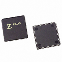
Z8F4822VS020SG Zilog, Z8F4822VS020SG Datasheet - Page 214

Z8F4822VS020SG
Manufacturer Part Number
Z8F4822VS020SG
Description
IC ENCORE MCU FLASH 48K 68PLCC
Manufacturer
Zilog
Series
Encore!® XP®r
Specifications of Z8F4822VS020SG
Core Processor
Z8
Core Size
8-Bit
Speed
20MHz
Connectivity
I²C, IrDA, SPI, UART/USART
Peripherals
Brown-out Detect/Reset, DMA, POR, PWM, WDT
Number Of I /o
46
Program Memory Size
48KB (48K x 8)
Program Memory Type
FLASH
Ram Size
4K x 8
Voltage - Supply (vcc/vdd)
3 V ~ 3.6 V
Data Converters
A/D 12x10b
Oscillator Type
Internal
Operating Temperature
0°C ~ 70°C
Package / Case
68-LCC (J-Lead)
Processor Series
Z8F482x
Core
eZ8
Data Bus Width
8 bit
Data Ram Size
4 KB
Interface Type
I2C, SPI, UART
Maximum Clock Frequency
20 MHz
Number Of Programmable I/os
46
Number Of Timers
4
Operating Supply Voltage
3 V to 3.6 V
Maximum Operating Temperature
+ 70 C
Mounting Style
SMD/SMT
Minimum Operating Temperature
0 C
On-chip Adc
10 bit, 12 Channel
Lead Free Status / RoHS Status
Lead free / RoHS Compliant
Eeprom Size
-
Lead Free Status / Rohs Status
Details
Other names
269-4273
Z8F4822VS020SG
Z8F4822VS020SG
Available stocks
Company
Part Number
Manufacturer
Quantity
Price
- Current page: 214 of 297
- Download datasheet (9Mb)
On-Chip Debugger Commands
Table 101. On-Chip Debugger Commands
PS019921-0308
Debug Command
Read OCD Revision
Read OCD Status
Register
Read Runtime Counter
Write OCD Control
Register
Read OCD Control
Register
Write Program Counter
Read Program Counter
Write Register
Read Register
Write Program Memory
Read Program Memory
Write Data Memory
Read Data Memory
The host communicates to the On-Chip Debugger by sending OCD commands using the
DBG interface. During normal operation, only a subset of the OCD commands are avail-
able. In DEBUG mode, all OCD commands become available unless the user code and
control registers are protected by programming the Read Protect Option Bit (RP). The
Read Protect Option Bit prevents the code in memory from being read out of the Z8
Encore! XP
commands are disabled.
mands. Each OCD command is described in detail in the bulleted list following
Table 101
(normal operation) and those commands that are disabled by programming the Read Pro-
tect Option Bit.
indicates those commands that operate when the device is not in DEBUG mode
Command
Byte
®
F64XX Series products. When this option is enabled, several of the OCD
0AH
0BH
0CH
0DH
02H
04H
05H
06H
07H
09H
00H
03H
08H
Table 101
Enabled when
NOT in DEBUG
mode?
contains a summary of the On-Chip Debugger com-
Yes
Yes
Yes
Yes
-
-
-
-
-
-
-
-
-
Disabled by
Read Protect Option Bit
Only writes of the Flash Memory Control
the Mass Erase command is allowed to
registers are allowed. Additionally, only
be written to the Flash Control register.
Z8 Encore! XP
Cannot clear DBGMODE bit
Product Specification
Disabled
Disabled
Disabled
Disabled
Disabled
Disabled
Disabled
-
-
-
-
®
On-Chip Debugger
F64XX Series
Table
101.
200
Related parts for Z8F4822VS020SG
Image
Part Number
Description
Manufacturer
Datasheet
Request
R

Part Number:
Description:
Communication Controllers, ZILOG INTELLIGENT PERIPHERAL CONTROLLER (ZIP)
Manufacturer:
Zilog, Inc.
Datasheet:

Part Number:
Description:
KIT DEV FOR Z8 ENCORE 16K TO 64K
Manufacturer:
Zilog
Datasheet:

Part Number:
Description:
KIT DEV Z8 ENCORE XP 28-PIN
Manufacturer:
Zilog
Datasheet:

Part Number:
Description:
DEV KIT FOR Z8 ENCORE 8K/4K
Manufacturer:
Zilog
Datasheet:

Part Number:
Description:
KIT DEV Z8 ENCORE XP 28-PIN
Manufacturer:
Zilog
Datasheet:

Part Number:
Description:
DEV KIT FOR Z8 ENCORE 4K TO 8K
Manufacturer:
Zilog
Datasheet:

Part Number:
Description:
CMOS Z8 microcontroller. ROM 16 Kbytes, RAM 256 bytes, speed 16 MHz, 32 lines I/O, 3.0V to 5.5V
Manufacturer:
Zilog, Inc.
Datasheet:

Part Number:
Description:
Low-cost microcontroller. 512 bytes ROM, 61 bytes RAM, 8 MHz
Manufacturer:
Zilog, Inc.
Datasheet:

Part Number:
Description:
Z8 4K OTP Microcontroller
Manufacturer:
Zilog, Inc.
Datasheet:

Part Number:
Description:
CMOS SUPER8 ROMLESS MCU
Manufacturer:
Zilog, Inc.
Datasheet:

Part Number:
Description:
SL1866 CMOSZ8 OTP Microcontroller
Manufacturer:
Zilog, Inc.
Datasheet:

Part Number:
Description:
SL1866 CMOSZ8 OTP Microcontroller
Manufacturer:
Zilog, Inc.
Datasheet:

Part Number:
Description:
OTP (KB) = 1, RAM = 125, Speed = 12, I/O = 14, 8-bit Timers = 2, Comm Interfaces Other Features = Por, LV Protect, Voltage = 4.5-5.5V
Manufacturer:
Zilog, Inc.
Datasheet:

Part Number:
Description:
Manufacturer:
Zilog, Inc.
Datasheet:


