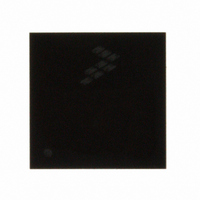
MC9S08GT8ACFDE Freescale Semiconductor, MC9S08GT8ACFDE Datasheet - Page 256

MC9S08GT8ACFDE
Manufacturer Part Number
MC9S08GT8ACFDE
Description
IC MCU 8K FLASH 1K RAM 48-QFN
Manufacturer
Freescale Semiconductor
Series
HCS08r
Datasheet
1.MC9S08GT8ACFBER.pdf
(300 pages)
Specifications of MC9S08GT8ACFDE
Core Processor
HCS08
Core Size
8-Bit
Speed
40MHz
Connectivity
I²C, SCI, SPI
Peripherals
LVD, POR, PWM, WDT
Number Of I /o
39
Program Memory Size
8KB (8K x 8)
Program Memory Type
FLASH
Ram Size
1K x 8
Voltage - Supply (vcc/vdd)
1.8 V ~ 3.6 V
Data Converters
A/D 8x10b
Oscillator Type
Internal
Operating Temperature
-40°C ~ 85°C
Package / Case
48-QFN
Processor Series
S08GT
Core
HCS08
Data Bus Width
8 bit
Data Ram Size
1 KB
Interface Type
I2C/SCI/SPI
Maximum Clock Frequency
40 MHz
Number Of Programmable I/os
39
Operating Supply Voltage
3.6 V
Maximum Operating Temperature
+ 85 C
Mounting Style
SMD/SMT
3rd Party Development Tools
EWS08
Development Tools By Supplier
M68EVB908GB60E, M68DEMO908GB60E
Minimum Operating Temperature
- 40 C
On-chip Adc
8-ch x 10-bit
For Use With
M68DEMO908GB60E - BOARD DEMO MC9S08GB60M68EVB908GB60E - BOARD EVAL FOR MC9S08GB60
Lead Free Status / RoHS Status
Lead free / RoHS Compliant
Eeprom Size
-
Lead Free Status / Rohs Status
Lead free / RoHS Compliant
- Current page: 256 of 300
- Download datasheet (2Mb)
Development Support
15.4.3.7
This register can be read or written at any time.
256
Reset
RWBEN
DBGEN
RWAEN
BRKEN
Field
ARM
RWA
RWB
TAG
W
7
6
5
4
3
2
1
0
R
DBGEN
Debug Module Enable — Used to enable the debug module. DBGEN cannot be set to 1 if the MCU is secure.
0 DBG disabled
1 DBG enabled
Arm Control — Controls whether the debugger is comparing and storing information in the FIFO. A write is used
to set this bit (and ARMF) and completion of a debug run automatically clears it. Any debug run can be manually
stopped by writing 0 to ARM or to DBGEN.
0 Debugger not armed
1 Debugger armed
Tag/Force Select — Controls whether break requests to the CPU will be tag or force type requests. If
BRKEN = 0, this bit has no meaning or effect.
0 CPU breaks requested as force type requests
1 CPU breaks requested as tag type requests
Break Enable — Controls whether a trigger event will generate a break request to the CPU. Trigger events can
cause information to be stored in the FIFO without generating a break request to the CPU. For an end trace, CPU
break requests are issued to the CPU when the comparator(s) and R/W meet the trigger requirements. For a
begin trace, CPU break requests are issued when the FIFO becomes full. TRGSEL does not affect the timing of
CPU break requests.
0 CPU break requests not enabled
1 Triggers cause a break request to the CPU
R/W Comparison Value for Comparator A — When RWAEN = 1, this bit determines whether a read or a write
access qualifies comparator A. When RWAEN = 0, RWA and the R/W signal do not affect comparator A.
0 Comparator A can only match on a write cycle
1 Comparator A can only match on a read cycle
Enable R/W for Comparator A — Controls whether the level of R/W is considered for a comparator A match.
0 R/W is not used in comparison A
1 R/W is used in comparison A
R/W Comparison Value for Comparator B — When RWBEN = 1, this bit determines whether a read or a write
access qualifies comparator B. When RWBEN = 0, RWB and the R/W signal do not affect comparator B.
0 Comparator B can match only on a write cycle
1 Comparator B can match only on a read cycle
Enable R/W for Comparator B — Controls whether the level of R/W is considered for a comparator B match.
0 R/W is not used in comparison B
1 R/W is used in comparison B
0
7
Debug Control Register (DBGC)
ARM
0
6
Table 15-4. DBGC Register Field Descriptions
Figure 15-7. Debug Control Register (DBGC)
MC9S08GT16A/GT8A Data Sheet, Rev. 1
TAG
0
5
BRKEN
0
4
Description
RWA
0
3
RWAEN
0
2
Freescale Semiconductor
RWB
1
0
RWBEN
0
0
Related parts for MC9S08GT8ACFDE
Image
Part Number
Description
Manufacturer
Datasheet
Request
R
Part Number:
Description:
Manufacturer:
Freescale Semiconductor, Inc
Datasheet:
Part Number:
Description:
Manufacturer:
Freescale Semiconductor, Inc
Datasheet:
Part Number:
Description:
Manufacturer:
Freescale Semiconductor, Inc
Datasheet:
Part Number:
Description:
Manufacturer:
Freescale Semiconductor, Inc
Datasheet:
Part Number:
Description:
Manufacturer:
Freescale Semiconductor, Inc
Datasheet:
Part Number:
Description:
Manufacturer:
Freescale Semiconductor, Inc
Datasheet:
Part Number:
Description:
Manufacturer:
Freescale Semiconductor, Inc
Datasheet:
Part Number:
Description:
Manufacturer:
Freescale Semiconductor, Inc
Datasheet:
Part Number:
Description:
Manufacturer:
Freescale Semiconductor, Inc
Datasheet:
Part Number:
Description:
Manufacturer:
Freescale Semiconductor, Inc
Datasheet:
Part Number:
Description:
Manufacturer:
Freescale Semiconductor, Inc
Datasheet:
Part Number:
Description:
Manufacturer:
Freescale Semiconductor, Inc
Datasheet:
Part Number:
Description:
Manufacturer:
Freescale Semiconductor, Inc
Datasheet:
Part Number:
Description:
Manufacturer:
Freescale Semiconductor, Inc
Datasheet:
Part Number:
Description:
Manufacturer:
Freescale Semiconductor, Inc
Datasheet:


