C8051F305-GMR Silicon Laboratories Inc, C8051F305-GMR Datasheet - Page 107
C8051F305-GMR
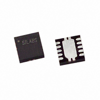
Manufacturer Part Number
C8051F305-GMR
Description
IC 8051 MCU 2K FLASH 11QFN
Manufacturer
Silicon Laboratories Inc
Series
C8051F30xr
Specifications of C8051F305-GMR
Core Processor
8051
Core Size
8-Bit
Speed
25MHz
Connectivity
SMBus (2-Wire/I²C), UART/USART
Peripherals
POR, PWM, WDT
Number Of I /o
8
Program Memory Size
2KB (2K x 8)
Program Memory Type
FLASH
Ram Size
256 x 8
Voltage - Supply (vcc/vdd)
2.7 V ~ 3.6 V
Oscillator Type
External
Operating Temperature
-40°C ~ 85°C
Package / Case
11-VQFN
For Use With
336-1444 - ADAPTER PROGRAM TOOLSTICK F300
Lead Free Status / RoHS Status
Lead free / RoHS Compliant
Eeprom Size
-
Data Converters
-
Available stocks
Company
Part Number
Manufacturer
Quantity
Price

Part Number:
C8051F305-GMR
Manufacturer:
SILICONLABS/芯科
Quantity:
20 000


Bits7–6: PCA0ME: PCA Module I/0 Enable Bits
Bit5:
Bit4:
Bit3:
Bit2:
Bit1:
Bit0:
Bit7:
Bits6–0: XSKP[6:0]: Crossbar Skip Enable Bits
R/W
R/W
Bit7
Bit7
—
PCA0ME
00: All PCA I/O unavailable at Port pins.
01: CEX0 routed to Port pin.
10: CEX0, CEX1 routed to Port pins.
11: CEX0, CEX1, CEX2 routed to Port pins.
CP0AOEN: Comparator0 Asynchronous Output Enable
0: Asynchronous CP0 unavailable at Port pin.
1: Asynchronous CP0 routed to Port pin.
CP0OEN: Comparator0 Output Enable
0: CP0 unavailable at Port pin.
1: CP0 routed to Port pin.
SYSCKE: /SYSCLK Output Enable
0: /SYSCLK unavailable at Port pin.
1: /SYSCLK output routed to Port pin.
SMB0OEN: SMBus I/O Enable
0: SMBus I/O unavailable at Port pins.
1: SDA, SCL routed to Port pins.
URX0EN: UART RX Enable
0: UART RX0 unavailable at Port pin.
1: UART RX0 routed to Port pin P0.5.
UTX0EN: UART TX Output Enable
0: UART TX0 unavailable at Port pin.
1: UART TX0 routed to Port pin P0.4.
UNUSED. Read = 0b; Write = don’t care.
These bits select Port pins to be skipped by the Crossbar Decoder. Port pins used as ana-
log inputs (for ADC or Comparator) or used as special functions (VREF input, external oscil-
lator circuit, CNVSTR input) should be skipped by the Crossbar.
0: Corresponding P0.n pin is not skipped by the Crossbar.
1: Corresponding P0.n pin is skipped by the Crossbar.
XSKP6
R/W
SFR Definition 12.2. XBR1: Port I/O Crossbar Register 1
R/W
SFR Definition 12.1. XBR0: Port I/O Crossbar Register 0
Bit6
Bit6
CP0AOEN CP0OEN SYSCKE SMB0OEN URX0EN UTX0EN 00000000
XSKP5
R/W
Bit5
R/W
Bit5
XSKP4
R/W
Bit4
R/W
Bit4
XSKP3
Rev. 2.9
R/W
Bit3
R/W
Bit3
XSKP2
R/W
Bit2
R/W
Bit2
C8051F300/1/2/3/4/5
XSKP1
R/W
Bit1
R/W
Bit1
XSKP0
R/W
Bit0
R/W
Bit0
SFR Address:
00000000
Reset Value
SFR Address:
Reset Value
0xE1
0xE2
107
Related parts for C8051F305-GMR
Image
Part Number
Description
Manufacturer
Datasheet
Request
R

Part Number:
Description:
SMD/C°/SINGLE-ENDED OUTPUT SILICON OSCILLATOR
Manufacturer:
Silicon Laboratories Inc
Part Number:
Description:
Manufacturer:
Silicon Laboratories Inc
Datasheet:
Part Number:
Description:
N/A N/A/SI4010 AES KEYFOB DEMO WITH LCD RX
Manufacturer:
Silicon Laboratories Inc
Datasheet:
Part Number:
Description:
N/A N/A/SI4010 SIMPLIFIED KEY FOB DEMO WITH LED RX
Manufacturer:
Silicon Laboratories Inc
Datasheet:
Part Number:
Description:
N/A/-40 TO 85 OC/EZLINK MODULE; F930/4432 HIGH BAND (REV E/B1)
Manufacturer:
Silicon Laboratories Inc
Part Number:
Description:
EZLink Module; F930/4432 Low Band (rev e/B1)
Manufacturer:
Silicon Laboratories Inc
Part Number:
Description:
I°/4460 10 DBM RADIO TEST CARD 434 MHZ
Manufacturer:
Silicon Laboratories Inc
Part Number:
Description:
I°/4461 14 DBM RADIO TEST CARD 868 MHZ
Manufacturer:
Silicon Laboratories Inc
Part Number:
Description:
I°/4463 20 DBM RFSWITCH RADIO TEST CARD 460 MHZ
Manufacturer:
Silicon Laboratories Inc
Part Number:
Description:
I°/4463 20 DBM RADIO TEST CARD 868 MHZ
Manufacturer:
Silicon Laboratories Inc
Part Number:
Description:
I°/4463 27 DBM RADIO TEST CARD 868 MHZ
Manufacturer:
Silicon Laboratories Inc
Part Number:
Description:
I°/4463 SKYWORKS 30 DBM RADIO TEST CARD 915 MHZ
Manufacturer:
Silicon Laboratories Inc
Part Number:
Description:
N/A N/A/-40 TO 85 OC/4463 RFMD 30 DBM RADIO TEST CARD 915 MHZ
Manufacturer:
Silicon Laboratories Inc
Part Number:
Description:
I°/4463 20 DBM RADIO TEST CARD 169 MHZ
Manufacturer:
Silicon Laboratories Inc