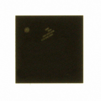
MC9S08QG84CFFE Freescale Semiconductor, MC9S08QG84CFFE Datasheet - Page 128

MC9S08QG84CFFE
Manufacturer Part Number
MC9S08QG84CFFE
Description
IC MCU 8BIT 8K FLASH 16-QFN
Manufacturer
Freescale Semiconductor
Series
HCS08r
Datasheet
1.MC9S08QG8CDTER.pdf
(314 pages)
Specifications of MC9S08QG84CFFE
Core Processor
HCS08
Core Size
8-Bit
Speed
20MHz
Connectivity
I²C, SCI, SPI
Peripherals
LVD, POR, PWM, WDT
Number Of I /o
12
Program Memory Size
8KB (8K x 8)
Program Memory Type
FLASH
Ram Size
512 x 8
Voltage - Supply (vcc/vdd)
1.8 V ~ 3.6 V
Data Converters
A/D 8x10b
Oscillator Type
Internal
Operating Temperature
-40°C ~ 85°C
Package / Case
16-QFN
Data Bus Width
8 bit
Data Ram Size
512 B
Interface Type
I2C, SCI, SPI
Maximum Clock Frequency
20 MHz
Number Of Programmable I/os
12
Number Of Timers
1
Maximum Operating Temperature
+ 85 C
Mounting Style
SMD/SMT
Minimum Operating Temperature
- 40 C
On-chip Adc
10 bit, 8 Channel
For Use With
DEMO9S08QG8E - BOARD DEMO FOR MC9S08QG8
Lead Free Status / RoHS Status
Lead free / RoHS Compliant
Eeprom Size
-
Lead Free Status / Rohs Status
Details
- Current page: 128 of 314
- Download datasheet (6Mb)
Analog-to-Digital Converter (S08ADC10V1)
126
ADLSMP
ADICLK
ADLPC
MODE
Field
ADIV
6:5
3:2
1:0
7
4
Reset:
W
R
Low Power Configuration — ADLPC controls the speed and power configuration of the successive
approximation converter. This is used to optimize power consumption when higher sample rates are not required.
0 High speed configuration
1 Low power configuration: {FC31}The power is reduced at the expense of maximum clock speed.
Clock Divide Select — ADIV select the divide ratio used by the ADC to generate the internal clock ADCK.
Table 9-6
Long Sample Time Configuration — ADLSMP selects between long and short sample time. This adjusts the
sample period to allow higher impedance inputs to be accurately sampled or to maximize conversion speed for
lower impedance inputs. Longer sample times can also be used to lower overall power consumption when
continuous conversions are enabled if high conversion rates are not required.
0 Short sample time
1 Long sample time
Conversion Mode Selection — MODE bits are used to select between 10- or 8-bit operation. See
Input Clock Select — ADICLK bits select the input clock source to generate the internal clock ADCK. See
Table
ADLPC
9-8.
7
0
shows the available clock configurations.
MODE
ADIV
00
01
10
11
00
01
10
11
0
6
Table 9-5. ADCCFG Register Field Descriptions
Figure 9-10. Configuration Register (ADCCFG)
MC9S08QG8 and MC9S08QG4 Data Sheet, Rev. 5
ADIV
8-bit conversion (N=8)
Reserved
10-bit conversion (N=10)
Reserved
Table 9-6. Clock Divide Select
Table 9-7. Conversion Modes
0
5
Divide Ratio
1
2
4
8
ADLSMP
0
4
Mode Description
Description
0
3
MODE
Input clock ÷ 2
Input clock ÷ 4
Input clock ÷ 8
Clock Rate
Input clock
0
2
Freescale Semiconductor
0
1
ADICLK
Table
0
0
9-7.
Related parts for MC9S08QG84CFFE
Image
Part Number
Description
Manufacturer
Datasheet
Request
R
Part Number:
Description:
Hcs08 Microcontrollers
Manufacturer:
Freescale Semiconductor, Inc
Datasheet:
Part Number:
Description:
Manufacturer:
Freescale Semiconductor, Inc
Datasheet:
Part Number:
Description:
Manufacturer:
Freescale Semiconductor, Inc
Datasheet:
Part Number:
Description:
Manufacturer:
Freescale Semiconductor, Inc
Datasheet:
Part Number:
Description:
Manufacturer:
Freescale Semiconductor, Inc
Datasheet:
Part Number:
Description:
Manufacturer:
Freescale Semiconductor, Inc
Datasheet:
Part Number:
Description:
Manufacturer:
Freescale Semiconductor, Inc
Datasheet:
Part Number:
Description:
Manufacturer:
Freescale Semiconductor, Inc
Datasheet:
Part Number:
Description:
Manufacturer:
Freescale Semiconductor, Inc
Datasheet:
Part Number:
Description:
Manufacturer:
Freescale Semiconductor, Inc
Datasheet:
Part Number:
Description:
Manufacturer:
Freescale Semiconductor, Inc
Datasheet:
Part Number:
Description:
Manufacturer:
Freescale Semiconductor, Inc
Datasheet:
Part Number:
Description:
Manufacturer:
Freescale Semiconductor, Inc
Datasheet:
Part Number:
Description:
Manufacturer:
Freescale Semiconductor, Inc
Datasheet:
Part Number:
Description:
Manufacturer:
Freescale Semiconductor, Inc
Datasheet:


