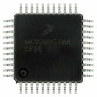
MC9S08GT8ACFBE Freescale Semiconductor, MC9S08GT8ACFBE Datasheet - Page 225

MC9S08GT8ACFBE
Manufacturer Part Number
MC9S08GT8ACFBE
Description
IC MCU 8K FLASH 1K RAM 44-QFP
Manufacturer
Freescale Semiconductor
Series
HCS08r
Datasheet
1.MC9S08GT8ACFBER.pdf
(300 pages)
Specifications of MC9S08GT8ACFBE
Core Processor
HCS08
Core Size
8-Bit
Speed
40MHz
Connectivity
I²C, SCI, SPI
Peripherals
LVD, POR, PWM, WDT
Number Of I /o
36
Program Memory Size
8KB (8K x 8)
Program Memory Type
FLASH
Ram Size
1K x 8
Voltage - Supply (vcc/vdd)
1.8 V ~ 3.6 V
Data Converters
A/D 8x10b
Oscillator Type
Internal
Operating Temperature
-40°C ~ 85°C
Package / Case
44-QFP
Processor Series
S08GT
Core
HCS08
Data Bus Width
8 bit
Data Ram Size
1 KB
Interface Type
I2C/SCI/SPI
Maximum Clock Frequency
40 MHz
Number Of Programmable I/os
36
Operating Supply Voltage
3.6 V
Maximum Operating Temperature
+ 85 C
Mounting Style
SMD/SMT
3rd Party Development Tools
EWS08
Development Tools By Supplier
M68EVB908GB60E, M68DEMO908GB60E
Minimum Operating Temperature
- 40 C
On-chip Adc
8-ch x 10-bit
For Use With
M68DEMO908GB60E - BOARD DEMO MC9S08GB60M68EVB908GB60E - BOARD EVAL FOR MC9S08GB60
Lead Free Status / RoHS Status
Lead free / RoHS Compliant
Eeprom Size
-
Lead Free Status / Rohs Status
Lead free / RoHS Compliant
Available stocks
Company
Part Number
Manufacturer
Quantity
Price
Company:
Part Number:
MC9S08GT8ACFBE
Manufacturer:
FREESCALE
Quantity:
1 600
Company:
Part Number:
MC9S08GT8ACFBE
Manufacturer:
Freescale Semiconductor
Quantity:
10 000
Company:
Part Number:
MC9S08GT8ACFBER
Manufacturer:
Freescale Semiconductor
Quantity:
10 000
- Current page: 225 of 300
- Download datasheet (2Mb)
14.2.1
The channel pins are used as the analog input pins of the ATD. Each pin is connected to an analog switch
which serves as the signal gate into the sample submodule.
14.2.2
These pins serve as the source for the high and low reference potentials for the converter. Separation from
the power supply pins accommodates the filtering necessary to achieve the accuracy of which the system
is capable.
14.2.3
These two pins are used to supply power and ground to the analog section of the ATD. Dedicated power
is required to isolate the sensitive analog circuitry from the normal levels of noise present on digital power
supplies.
14.3
The ATD has seven registers that control ATD functions.
Refer to the direct-page register summary in the memory chapter of this data sheet for the absolute address
assignments for all ATD registers. This section refers to registers and control bits only by their names. A
Freescale-provided equate or header file is used to translate these names into the appropriate absolute
addresses.
14.3.1
Writes to the ATD control register will abort the current conversion, but will not start a new conversion.
Freescale Semiconductor
Register Definition
ADP7–ADP0 — Channel Input Pins
V
V
ATD Control (ATDC)
REFH
DDAD
V
must be at the same potential.
DDAD1
, V
, V
REFL
SSAD
and V
AD7–AD0
DD
— ATD Reference Pins
V
— ATD Supply Pins
V
V
Name
V
DDAD
REFH
SSAD
REFL
must be at the same potential. Likewise, V
MC9S08GT16A/GT8A Data Sheet, Rev. 1
Table 14-1. Signal Properties
High reference voltage for ATD converter
Low reference voltage for ATD converter
ATD ground supply voltage
ATD power supply voltage
NOTE
Channel input pins
Function
Analog-to-Digital Converter (S08ATDV3)
SSAD1
and V
SS
225
Related parts for MC9S08GT8ACFBE
Image
Part Number
Description
Manufacturer
Datasheet
Request
R
Part Number:
Description:
Manufacturer:
Freescale Semiconductor, Inc
Datasheet:
Part Number:
Description:
Manufacturer:
Freescale Semiconductor, Inc
Datasheet:
Part Number:
Description:
Manufacturer:
Freescale Semiconductor, Inc
Datasheet:
Part Number:
Description:
Manufacturer:
Freescale Semiconductor, Inc
Datasheet:
Part Number:
Description:
Manufacturer:
Freescale Semiconductor, Inc
Datasheet:
Part Number:
Description:
Manufacturer:
Freescale Semiconductor, Inc
Datasheet:
Part Number:
Description:
Manufacturer:
Freescale Semiconductor, Inc
Datasheet:
Part Number:
Description:
Manufacturer:
Freescale Semiconductor, Inc
Datasheet:
Part Number:
Description:
Manufacturer:
Freescale Semiconductor, Inc
Datasheet:
Part Number:
Description:
Manufacturer:
Freescale Semiconductor, Inc
Datasheet:
Part Number:
Description:
Manufacturer:
Freescale Semiconductor, Inc
Datasheet:
Part Number:
Description:
Manufacturer:
Freescale Semiconductor, Inc
Datasheet:
Part Number:
Description:
Manufacturer:
Freescale Semiconductor, Inc
Datasheet:
Part Number:
Description:
Manufacturer:
Freescale Semiconductor, Inc
Datasheet:
Part Number:
Description:
Manufacturer:
Freescale Semiconductor, Inc
Datasheet:


