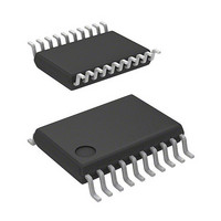
R5F21294SNSP#U0 Renesas Electronics America, R5F21294SNSP#U0 Datasheet - Page 80

R5F21294SNSP#U0
Manufacturer Part Number
R5F21294SNSP#U0
Description
MCU 3/5V 16K+2K 20PIN-SSOP
Manufacturer
Renesas Electronics America
Series
M16C™ M16C/R8C/Tiny/29r
Datasheet
1.R5F21282SNSPU0.pdf
(473 pages)
Specifications of R5F21294SNSP#U0
Core Processor
R8C
Core Size
16-Bit
Speed
20MHz
Connectivity
I²C, LIN, SIO, SSU, UART/USART
Peripherals
LED, POR, Voltage Detect, WDT
Number Of I /o
13
Program Memory Size
16KB (16K x 8)
Program Memory Type
FLASH
Ram Size
1K x 8
Voltage - Supply (vcc/vdd)
2.2 V ~ 5.5 V
Data Converters
A/D 4x10b
Oscillator Type
Internal
Operating Temperature
-20°C ~ 85°C
Package / Case
20-SSOP
Lead Free Status / RoHS Status
Lead free / RoHS Compliant
Eeprom Size
-
Available stocks
Company
Part Number
Manufacturer
Quantity
Price
- Current page: 80 of 473
- Download datasheet (5Mb)
R8C/28 Group, R8C/29 Group
Rev.2.10
REJ09B0279-0210
7.4
Table 7.4
X: 0 or 1
NOTE:
Table 7.5
X: 0 or 1
NOTE:
Table 7.6
X: 0 or 1
Table 7.7
X: 0 or 1
NOTE:
Tables 7.4 to 7.25 list the port settings.
Register
Register
Register
Register
Setting
Setting
Setting
Setting
Value
1. Pulled up by setting the PU02 bit in the PUR0 register to 1.
Value
1. Pulled up by setting the PU02 bit in the PUR0 register to 1.
Value
Value
1. Pulled up by setting the PU02 bit in the PUR0 register to 1.
Bit
Bit
Bit
Bit
Port Settings
Sep 26, 2008
TRCOER
PD1_1 KI1EN
PD1_2 KI2EN
PD1
PD1
PD1_0
X
X
0
1
0
0
0
0
1
0
0
0
PD1
EA
Port P1_0/KI0/AN8
Port P1_1/KI1/AN9/TRCIOA/TRCTRG
Port P1_2/KI2/AN10/TRCIOB
TRCIOA Pin Setting
0
0
1
1
0
1
0
0
KIEN
KIEN
0
0
0
1
0
0
0
0
0
1
0
0
TRCMR
PWM2
KI0EN
KIEN
1
1
0
Page 61 of 441
0
0
1
0
Other than TRCIOA usage conditions
Other than TRCIOA usage conditions
Other than TRCIOA usage conditions
Other than TRCIOA usage conditions
Other than TRCIOB usage conditions
Other than TRCIOB usage conditions
Other than TRCIOB usage conditions
Other than TRCIOB usage conditions
Refer to Table 7.6 TRCIOA Pin
Refer to Table 7.6 TRCIOA Pin
Refer to Table 7.8 TRCIOB Pin
Refer to Table 7.8 TRCIOB Pin
IOA2
X
0
0
1
CH2
Timer RC Setting
Timer RC Setting
X
X
X
1
Other than above
Setting
Setting
Setting
Setting
TRCIOR0
−
−
IOA1
X
X
0
1
CH1
X
X
X
0
ADCON0
IOA0
X
X
X
1
CH0
X
X
X
0
CH2 CH1 CH0 ADGSEL0
CH2
TCEG1
X
X
1
X
X
X
X
X
X
X
X
1
X
X
X
X
0
1
ADGSEL0
TRCCR2
CH1
X
X
X
X
X
X
X
X
1
1
X
X
X
X
X
0
ADCON0
ADCON0
TCEG0
CH0 ADGSEL0
X
X
X
X
1
X
X
X
X
X
X
0
X
X
X
X
X
1
Input port
Output port
KI0 input
A/D converter input (AN8)
Timer waveform output
(output compare function)
Timer mode (input capture function)
PWM2 mode TRCTRG input
Other than TRCIOA usage conditions
X
X
X
X
X
1
(1)
X
X
X
X
X
1
(1)
7. Programmable I/O Ports
Input port
Output port
A/D converter input (AN10)
KI2 input
TRCIOB output
TRCIOB input
Input port
Output port
A/D converter input (AN9)
KI1 input
TRCIOA output
TRCIOA input
Function
Function
(1)
Function
Function
(1)
(1)
(1)
(1)
(1)
Related parts for R5F21294SNSP#U0
Image
Part Number
Description
Manufacturer
Datasheet
Request
R

Part Number:
Description:
KIT STARTER FOR M16C/29
Manufacturer:
Renesas Electronics America
Datasheet:

Part Number:
Description:
KIT STARTER FOR R8C/2D
Manufacturer:
Renesas Electronics America
Datasheet:

Part Number:
Description:
R0K33062P STARTER KIT
Manufacturer:
Renesas Electronics America
Datasheet:

Part Number:
Description:
KIT STARTER FOR R8C/23 E8A
Manufacturer:
Renesas Electronics America
Datasheet:

Part Number:
Description:
KIT STARTER FOR R8C/25
Manufacturer:
Renesas Electronics America
Datasheet:

Part Number:
Description:
KIT STARTER H8S2456 SHARPE DSPLY
Manufacturer:
Renesas Electronics America
Datasheet:

Part Number:
Description:
KIT STARTER FOR R8C38C
Manufacturer:
Renesas Electronics America
Datasheet:

Part Number:
Description:
KIT STARTER FOR R8C35C
Manufacturer:
Renesas Electronics America
Datasheet:

Part Number:
Description:
KIT STARTER FOR R8CL3AC+LCD APPS
Manufacturer:
Renesas Electronics America
Datasheet:

Part Number:
Description:
KIT STARTER FOR RX610
Manufacturer:
Renesas Electronics America
Datasheet:

Part Number:
Description:
KIT STARTER FOR R32C/118
Manufacturer:
Renesas Electronics America
Datasheet:

Part Number:
Description:
KIT DEV RSK-R8C/26-29
Manufacturer:
Renesas Electronics America
Datasheet:

Part Number:
Description:
KIT STARTER FOR SH7124
Manufacturer:
Renesas Electronics America
Datasheet:

Part Number:
Description:
KIT STARTER FOR H8SX/1622
Manufacturer:
Renesas Electronics America
Datasheet:

Part Number:
Description:
KIT DEV FOR SH7203
Manufacturer:
Renesas Electronics America
Datasheet:


