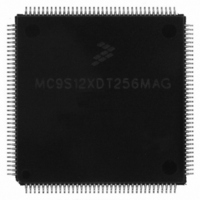
MC9S12XDT256MAG Freescale Semiconductor, MC9S12XDT256MAG Datasheet - Page 422

MC9S12XDT256MAG
Manufacturer Part Number
MC9S12XDT256MAG
Description
IC MCU 256K FLASH 144-LQFP
Manufacturer
Freescale Semiconductor
Series
HCS12r
Datasheet
1.MC9S12XD64CAA.pdf
(1348 pages)
Specifications of MC9S12XDT256MAG
Core Processor
HCS12X
Core Size
16-Bit
Speed
80MHz
Connectivity
CAN, EBI/EMI, I²C, IrDA, LIN, SCI, SPI
Peripherals
LVD, POR, PWM, WDT
Number Of I /o
119
Program Memory Size
256KB (256K x 8)
Program Memory Type
FLASH
Eeprom Size
4K x 8
Ram Size
16K x 8
Voltage - Supply (vcc/vdd)
2.35 V ~ 5.5 V
Data Converters
A/D 24x10b
Oscillator Type
External
Operating Temperature
-40°C ~ 125°C
Package / Case
144-LQFP
Processor Series
S12XD
Core
HCS12
Data Bus Width
16 bit
Data Ram Size
16 KB
Interface Type
CAN/I2C/SCI/SPI
Maximum Clock Frequency
40 MHz
Number Of Programmable I/os
119
Number Of Timers
12
Operating Supply Voltage
0 V to 5.5 V
Maximum Operating Temperature
+ 125 C
Mounting Style
SMD/SMT
3rd Party Development Tools
EWHCS12
Development Tools By Supplier
EVB9S12XDP512E
Minimum Operating Temperature
- 40 C
On-chip Adc
2 (24-ch x 10-bit)
Lead Free Status / RoHS Status
Lead free / RoHS Compliant
Available stocks
Company
Part Number
Manufacturer
Quantity
Price
Company:
Part Number:
MC9S12XDT256MAG
Manufacturer:
Freescale Semiconductor
Quantity:
10 000
- Current page: 422 of 1348
- Download datasheet (8Mb)
Chapter 10 Freescale’s Scalable Controller Area Network (S12MSCANV3)
10.3
This section provides a detailed description of all registers accessible in the MSCAN.
10.3.1
Figure 10-3
register address results from the addition of base address and address offset. The base address is
determined at the MCU level and can be found in the MCU memory map description. The address offset
is defined at the module level.
The MSCAN occupies 64 bytes in the memory space. The base address of the MSCAN module is
determined at the MCU level when the MCU is defined. The register decode map is fixed and begins at the
first address of the module address offset.
The detailed register descriptions follow in the order they appear in the register map.
422
CANCTL0
CANCTL1
Register
0x0000
0x0001
Name
Memory Map and Register Definition
Module Memory Map
gives an overview on all registers and their individual bits in the MSCAN memory map. The
R
W
R
W
TXCAN
RXFRM
CAN_H
CANE
Bit 7
CAN node 1
CAN Controller
(MSCAN)
Transceiver
MCU
= Unimplemented or Reserved
CLKSRC
RXACT
Figure 10-3. MSCAN Register Summary
6
MC9S12XDP512 Data Sheet, Rev. 2.21
CAN_L
RXCAN
Figure 10-2. CAN System
LOOPB
CSWAI
5
CAN Bus
LISTEN
SYNCH
CAN node 2
4
BORM
TIME
3
CAN node n
u = Unaffected
WUPM
WUPE
2
Freescale Semiconductor
SLPRQ
SLPAK
1
INITRQ
INITAK
Bit 0
Related parts for MC9S12XDT256MAG
Image
Part Number
Description
Manufacturer
Datasheet
Request
R

Part Number:
Description:
16-BIT MICROPROCESSOR FAMILY
Manufacturer:
FREESCALE [Freescale Semiconductor, Inc]
Datasheet:
Part Number:
Description:
Manufacturer:
Freescale Semiconductor, Inc
Datasheet:
Part Number:
Description:
Manufacturer:
Freescale Semiconductor, Inc
Datasheet:
Part Number:
Description:
Manufacturer:
Freescale Semiconductor, Inc
Datasheet:
Part Number:
Description:
Manufacturer:
Freescale Semiconductor, Inc
Datasheet:
Part Number:
Description:
Manufacturer:
Freescale Semiconductor, Inc
Datasheet:
Part Number:
Description:
Manufacturer:
Freescale Semiconductor, Inc
Datasheet:
Part Number:
Description:
Manufacturer:
Freescale Semiconductor, Inc
Datasheet:
Part Number:
Description:
Manufacturer:
Freescale Semiconductor, Inc
Datasheet:
Part Number:
Description:
Manufacturer:
Freescale Semiconductor, Inc
Datasheet:
Part Number:
Description:
Manufacturer:
Freescale Semiconductor, Inc
Datasheet:
Part Number:
Description:
Manufacturer:
Freescale Semiconductor, Inc
Datasheet:
Part Number:
Description:
Manufacturer:
Freescale Semiconductor, Inc
Datasheet:
Part Number:
Description:
Manufacturer:
Freescale Semiconductor, Inc
Datasheet:
Part Number:
Description:
Manufacturer:
Freescale Semiconductor, Inc
Datasheet:


