MC9S12DG128MFUE Freescale Semiconductor, MC9S12DG128MFUE Datasheet - Page 63
MC9S12DG128MFUE
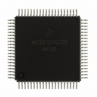
Manufacturer Part Number
MC9S12DG128MFUE
Description
IC MCU 128K FLASH 80-QFP
Manufacturer
Freescale Semiconductor
Series
HCS12r
Datasheet
1.MC9S12DG128CFUER.pdf
(128 pages)
Specifications of MC9S12DG128MFUE
Core Processor
HCS12
Core Size
16-Bit
Speed
25MHz
Connectivity
CAN, I²C, SCI, SPI
Peripherals
PWM, WDT
Number Of I /o
59
Program Memory Size
128KB (128K x 8)
Program Memory Type
FLASH
Eeprom Size
2K x 8
Ram Size
8K x 8
Voltage - Supply (vcc/vdd)
2.35 V ~ 5.25 V
Data Converters
A/D 16x10b
Oscillator Type
Internal
Operating Temperature
-40°C ~ 125°C
Package / Case
80-QFP
Lead Free Status / RoHS Status
Lead free / RoHS Compliant
Available stocks
Company
Part Number
Manufacturer
Quantity
Price

Company:
Part Number:
MC9S12DG128MFUE
Manufacturer:
Freescale Semiconductor
Quantity:
10 000
Part Number:
MC9S12DG128MFUE 1L59W
Manufacturer:
FREESCALE
Quantity:
20 000


Freescale Semiconductor, Inc.
MC9S12DT128B Device User Guide — V01.09
2.3.36 PM4 / BF_PSYN / RXCAN0 / RXCAN4/ MOSI0 — Port M I/O Pin 4
PM4 is a general purpose input or output pin. It can be configured as the correct synchronisation pulse
reception/transmission output pulse pin of Byteflight. It can be configured as the receive pin RXCAN of
the Motorola Scalable Controller Area Network controllers 0 or 4 (CAN0 or CAN4). It can be configured
as the master output (during master mode) or slave input pin (during slave mode) MOSI for the Serial
Peripheral Interface 0 (SPI0).
2.3.37 PM3 / TX_BF / TXCAN1 / TXCAN0 / SS0 — Port M I/O Pin 3
PM3 is a general purpose input or output pin. It can be configured as the transmit pinTX_BF of Byteflight.
It can be configured as the transmit pin TXCAN of the Motorola Scalable Controller Area Network
controllers 1 or 0 (CAN1 or CAN0). It can be configured as the slave select pin SS of the Serial Peripheral
Interface 0 (SPI0).
2.3.38 PM2 / RX_BF / RXCAN1 / RXCAN0 / MISO0 — Port M I/O Pin 2
PM2 is a general purpose input or output pin. It can be configured as the receive pin RX_BF of Byteflight.
It can be configured as the receive pin RXCAN of the Motorola Scalable Controller Area Network
controllers 1 or 0 (CAN1 or CAN0). It can be configured as the master input (during master mode) or slave
output pin (during slave mode) MISO for the Serial Peripheral Interface 0 (SPI0).
2.3.39 PM1 / TXCAN0 / TXB — Port M I/O Pin 1
PM1 is a general purpose input or output pin. It can be configured as the transmit pin TXCAN of the
Motorola Scalable Controller Area Network controller 0 (CAN0). It can be configured as the transmit pin
TXB of the BDLC.
2.3.40 PM0 / RXCAN0 / RXB — Port M I/O Pin 0
PM0 is a general purpose input or output pin. It can be configured as the receive pin RXCAN of the
Motorola Scalable Controller Area Network controller 0 (CAN0). It can be configured as the receive pin
RXB of the BDLC.
2.3.41 PP7 / KWP7 / PWM7 — Port P I/O Pin 7
PP7 is a general purpose input or output pin. It can be configured to generate an interrupt causing the MCU
to exit STOP or WAIT mode. It can be configured as Pulse Width Modulator (PWM) channel 7 output.
2.3.42 PP6 / KWP6 / PWM6 — Port P I/O Pin 6
PP6 is a general purpose input or output pin. It can be configured to generate an interrupt causing the MCU
to exit STOP or WAIT mode. It can be configured as Pulse Width Modulator (PWM) channel 6 output.
For More Information On This Product,
Go to: www.freescale.com
Related parts for MC9S12DG128MFUE
Image
Part Number
Description
Manufacturer
Datasheet
Request
R

Part Number:
Description:
Manufacturer:
Freescale Semiconductor, Inc
Datasheet:
Part Number:
Description:
Manufacturer:
Freescale Semiconductor, Inc
Datasheet:
Part Number:
Description:
Manufacturer:
Freescale Semiconductor, Inc
Datasheet:
Part Number:
Description:
Manufacturer:
Freescale Semiconductor, Inc
Datasheet:
Part Number:
Description:
Manufacturer:
Freescale Semiconductor, Inc
Datasheet:
Part Number:
Description:
Manufacturer:
Freescale Semiconductor, Inc
Datasheet:
Part Number:
Description:
Manufacturer:
Freescale Semiconductor, Inc
Datasheet:
Part Number:
Description:
Manufacturer:
Freescale Semiconductor, Inc
Datasheet:
Part Number:
Description:
Manufacturer:
Freescale Semiconductor, Inc
Datasheet:
Part Number:
Description:
Manufacturer:
Freescale Semiconductor, Inc
Datasheet:
Part Number:
Description:
Manufacturer:
Freescale Semiconductor, Inc
Datasheet:
Part Number:
Description:
Manufacturer:
Freescale Semiconductor, Inc
Datasheet:
Part Number:
Description:
Manufacturer:
Freescale Semiconductor, Inc
Datasheet:
Part Number:
Description:
Manufacturer:
Freescale Semiconductor, Inc
Datasheet:
Part Number:
Description:
Manufacturer:
Freescale Semiconductor, Inc
Datasheet: