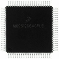
MC9S12C64CFUE Freescale Semiconductor, MC9S12C64CFUE Datasheet

MC9S12C64CFUE
Specifications of MC9S12C64CFUE
Available stocks
Related parts for MC9S12C64CFUE
MC9S12C64CFUE Summary of contents
Page 1
... INT (interrupt control) — BDM (background debug mode) — DBG12 (enhanced debug12 module including breakpoints and change-of-flow trace buffer) — Multiplexed Expansion Bus (available only in 80-pin package version) © Freescale Semiconductor, Inc., 2005, 2006. All rights reserved. MC9S12CFAMPB Rev. 5, 03/2006 ...
Page 2
... Programmable period and duty cycle — 8-bit 6-channel or 16-bit 3-channel — Separate control for each pulse width and duty cycle — Center-aligned or left-aligned outputs — Programmable clock select logic with a wide range of frequencies — Fast emergency shutdown input 2 MC9S12C-Family, Rev. 5 Freescale Semiconductor ...
Page 3
... I/O lines with 5V input and drive capability — dedicated 5V input only lines (IRQ, XIRQ) — 5V A/D converter inputs and 5V I/O • Development Support — Single-wire background debug™ mode (BDM) — On-chip hardware breakpoints — Enhanced DBG12 debug features Freescale Semiconductor MC9S12C-Family, Rev. 5 Features 3 ...
Page 4
... Freescale Semiconductor I ...
Page 5
... Interrupt capability ( IRQ, XIRQ) • For 52 Pin Versions: — Port input only PAD = 8. — 5 inputs provide Interrupt capability ( IRQ, XIRQ) • For 48 Pin Versions: — Port input only PAD = 8. — 3 inputs provide Interrupt capability ( IRQ, XIRQ) Freescale Semiconductor MC9S12C-Family, Rev. 5 Pin Out Explanations 5 ...
Page 6
... AN3 PAD3 AN4 PAD4 AN5 PAD5 AN6 PAD6 AN7 PAD7 PT0 PT1 MUX PT2 PT3 PT4 PT5 PT6 PT7 PP0 PP1 PP2 PP3 PP4 PP5 PP6 PP7 PJ6 PJ7 PS0 PS1 PS2 PS3 PM0 PM1 PM2 PM3 PM4 PM5 Freescale Semiconductor ...
Page 7
... The figure shows a useful map, which is not the map out of reset. After reset the map is: $0000 - $03FF: Register Space $0000 - $0FFF: 4K RAM (only 3K visible $0400 - $0FFF) Flash Erase Sector Size is 1024 Bytes Figure 2. MCxS12C128 User Configurable Memory Map Freescale Semiconductor EXT VECTORS VECTORS EXPANDED ...
Page 8
... Mappable to any 2K Boundary $0000 16K Fixed Flash EEPROM/ROM $3FFF $3000 4K Bytes RAM $3FFF Mappable to any 4K Boundary $4000 16K Fixed Flash EEPROM/ROM $7FFF $8000 16K Page Window 6 * 16K Flash EEPROM/ROM Pages $BFFF 16K Fixed Flash EEPROM/ROM $C000 $FFFF $FF00 BDM (If Active) $FFFF Freescale Semiconductor ...
Page 9
... The figure shows a useful map, which is not the map out of reset. After reset the map is: $0000 - $03FF: Register Space $0000 - $0FFF: 4K RAM (only 3K visible $0400 - $0FFF) Flash Erase Sector Size is 512 Bytes Figure 4. MCxS12C64 User Configurable Memory Map Freescale Semiconductor EXT VECTORS VECTORS EXPANDED ...
Page 10
... EXPANDED SPECIAL SINGLE CHIP MC9S12C-Family, Rev. 5 $0000 1K Register Space $03FF Mappable to any 2K Boundary $3800 2K Bytes RAM $3FFF Mappable to any 2K Boundary $8000 16K Page Window 2 * 16K Flash EEPROM/ROM Pages $BFFF 16K Fixed Flash EEPROM/ROM $C000 $FFFF $FF00 BDM (If Active) $FFFF Freescale Semiconductor ...
Page 11
... The figure shows a useful map, which is not the map out of reset. After reset the map is: $0000 - $03FF: Register Space $0800 - $0FFF: 2K RAM Flash Erase Sector Size is 512 Bytes Figure 6. MCxS12C16 User Configurable Memory Map Freescale Semiconductor EXT VECTORS VECTORS EXPANDED SPECIAL SINGLE CHIP MC9S12C-Family, Rev ...
Page 12
... EXPANDED SPECIAL SINGLE CHIP MC9S12C-Family, Rev. 5 $0000 1K Register Space $03FF Mappable to any 2K Boundary $3C00 1K Bytes RAM $3FFF Mappable to any 2K Boundary $8000 16K Page Window 1 * 16K Flash EEPROM/ROM Page $BFFF 16K Fixed Flash EEPROM/ROM $C000 $FFFF $FF00 BDM (If Active) $FFFF Freescale Semiconductor ...
Page 13
... ADDR4/DATA4/PB4 20 Signals shown in Bold are not available on the Pin Package Signals shown in Bold Italic are available in the 52, but not the 48 Pin Package Figure 8. Pin Assignments for 80-pin QFP for MC9S12C-Family Freescale Semiconductor MC9S12C-Family 80 QFP !!! Pin-out is Subject to Change !!! MC9S12C-Family, Rev. 5 Pin Assignments ...
Page 14
... IOC6/PT6 11 IOC7/PT7 12 MODC/BKGD 13 PB4 * Signals shown in Bold are not available on the 48 Pin Package Figure 9. Pin Assignments for 52-pin LQFP for MC9S12C-Family MC9S12C-Family 33 52 LQFP MC9S12C-Family, Rev. 5 VRH VDDA PAD07/AN07 PAD06/AN06 PAD05/AN05 PAD04/AN04 PAD03/AN03 PAD02/AN02 PAD01/AN01 PAD00/AN00 PA2 PA1 PA0 Freescale Semiconductor ...
Page 15
... PW0/IOC0/PT0 1 PW1/IOC1/PT1 2 PW2/IOC2/PT2 3 PW3/IOC3/PT3 4 VDD1 5 VSS1 6 PW4/IOC4/PT4 7 8 IOC5/PT5 9 IOC6/PT6 10 IOC7/PT7 11 MODC/BKGD 12 PB4 Figure 10. Pin Assignments for 48-pin LQFP for MC9S12C-Family Freescale Semiconductor MC9S12C-Family 48 LQFP MC9S12C-Family, Rev. 5 Pin Assignments VRH VDDA PAD07/AN07 PAD06/AN06 PAD05/AN05 PAD04/AN04 PAD03/AN03 PAD02/AN02 PAD01/AN01 PAD00/AN00 PA0 XIRQ/PE0 ...
Page 16
... Package Mechanical Information 7 Package Mechanical Information Refer to the following pages for detailed package dimensions. 16 MC9S12C-Family, Rev. 5 Freescale Semiconductor ...
Page 17
... Freescale Semiconductor MC9S12C-Family, Rev. 5 Package Mechanical Information 17 ...
Page 18
... Package Mechanical Information 18 MC9S12C-Family, Rev. 5 Freescale Semiconductor ...
Page 19
... Freescale Semiconductor MC9S12C-Family, Rev. 5 Package Mechanical Information 19 ...
Page 20
... Package Mechanical Information 20 MC9S12C-Family, Rev. 5 Freescale Semiconductor ...
Page 21
... Freescale Semiconductor MC9S12C-Family, Rev. 5 Package Mechanical Information 21 ...
Page 22
... Package Mechanical Information 22 MC9S12C-Family, Rev. 5 Freescale Semiconductor ...
Page 23
... Freescale Semiconductor MC9S12C-Family, Rev. 5 Package Mechanical Information 23 ...
Page 24
... Package Mechanical Information 24 MC9S12C-Family, Rev. 5 Freescale Semiconductor ...
Page 25
... Freescale Semiconductor MC9S12C-Family, Rev. 5 Package Mechanical Information 25 ...
Page 26
... Freescale Semiconductor product could create a situation where personal injury or death may occur. Should Buyer ...


